Fujitsu’s CS81, a 0.18µm (0.13µm L
eff
) standard-cell
product, is based on Fujitsu’s state-of-the-art CMOS
process technology, a deep sub-micron process designed
for today’s high-density and low-power SOC products.
The cell library, which is optimized for synthesis-based
designs, has accurate timing and power-characterized
data, cell areas, and statistical wire-load models. The
CS81 standard-cell library contains both high-perfor-
mance and high-density cells, giving designers the
option of combining both types of standard cell blocks
on the same chip. The CS81 library supports popular
third-party tools and data-exchange file standards.
The CS81 chip cores can operate at 1.8V to 1.1V. The
I/Os, operating at 1.8V, 2.5V, 3.3V, or 5V tolerance, can
conveniently interface with various types of devices.
Interface options include low-swing, high-speed I/Os
and high-speed bus interface I/Os.
Both inline and staggered I/O pad configurations are
available. Inline pads are available in both 70µm and
44µm pad pitch. The 70µm pads are wire bonded,
whereas the 44µm pads are used with TAB. The 66µm
wire-bond stagger pads can be used for optimizing the
die area of pad-limited designs.
CS81 Series Standard Cell
0.18µm CMOS Technology
Features
▼
Description
▼
In addition to the traditional QFP packages, the CS81
family is available in TAB, EBGA, FBGA, and Flip-
chip BGA packages.
CS81 offers a rich set of ADCs and DACs, PLLs, high-
speed RAMs and ROMs, as well as a variety of other
embedded functions. The following blocks will be avail-
able in the near future:
• Special high-speed I/Os:
T-LVTTL, P-CML, LVDS, SSTL, and HSTL
• Special-purpose Interfaces:
PCI, AGP, and USB
Design Methodology
Fujitsu’s design methodology ensures first-time silicon suc-
cess by integrating proprietary point tools with popular,
sign-off-quality, industry-standard CAD tools such as:
• Logic design rule checker
• Delay calculator
• Quasi 3-D parasitic extraction tool
Fujitsu’s clock-driven design methodology is devised for low
power and low skew. The methodology identifies the best-
suited clock distribution strategy for a given design and
CS81
(1.8V)
High-Speed
Devices
T-LVTTL
P-CML
LVDS
SSTL
HSTL
ADC/DAC
2.5V
CMOS
AGP USBPCI
AGP USB DevicesPCI Bus
3.3V
CMOS
High-Speed
Interface
Analog
Interface
2.5V CMOS
2.5V Device
3.3V Device
3.3V TTL
1.8V Device
1.8V CMOS
1.8V
CMOS
PLL
Clock Input
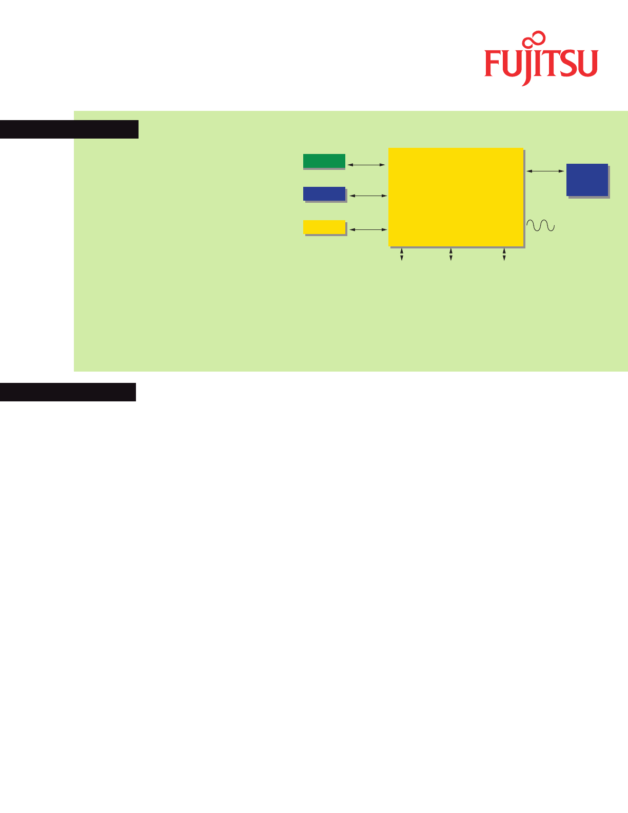
CS81 I/O Interface Capabilities
• 0.13µm effective channel length
• 3 to 5 layers of metal interconnects
• Very high density: 110K raw gates/mm
2
• Up to 28 million gates
• Core power supply voltage: 1.8V to 1.1V
• 5 nW/gate/MHz power dissipation at 1.1V
• 11 ps gate delay at 1.8V and 1 fan-out
• Junction temperature range: –40 to +125°C
• I/Os: 3.3V, 2.5V, 1.8V, 5V tolerant
• High-density diffused RAMs and ROMs
• High-speed mixed-signal macros
• Analog PLLs
• Wide selection of advanced packaging options
• Proven design methodology and tool support
• Two cell libraries: high-performance and
high-density
