


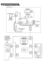
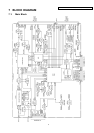
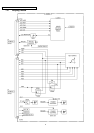
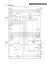
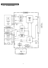
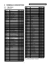
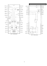
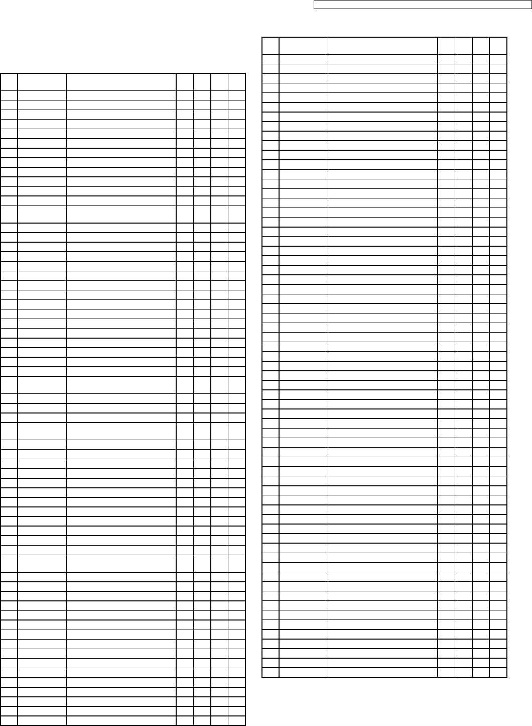
8.1. Main Block
IC701 : C2CBKA000001
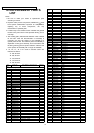
Pin
No.
Port Descriptions I/O
(V)
FM
(V)
AM
(V)
CD
(V)
1 /RSTOUT Not used - - - -
2 NMI (Connecting to GND) - 0 0 0
3 VSS GND - 0 0 0
4 VDD +5V power supply - 4.8 4.8 4.8
5 ILL1 Illumi control O 0 0 0
6 ILL2 Iiiumi. control O 2 2 1.2
7 TUNER1.ON Radio power on/off O 4.8 4.8 4.8
8 TUNER2.ON Radio power on/off O 4.8 4.8 4.8
9 DSP.PWN DSP power cont. O 0 0 0
10 LCD.ADR LCD address O 0 0 0
11 LCDRST LCD reset O 4.8 4.8 4.8
12 LCD/E2.CLK LCD/SEC. data shift clock O 0 0 0
13 LCD/E2.DT.I
N
LCD/SEC. serial data O 0 0 0
14 E2.DT.OUT Security data I 0 0 0
15 E2.CS Security IC selection O 0 0 0
16 AUDIO.ON Audio power on/off O 4.8 4.8 4.8
17 VSS GND - 0 0 0
18 VDD +5V power supply - 4.8 4.8 4.8
19 I2C.DATA DSP/AF.SW data O 4.8 4.8 4.8
20 I2C.CLK Data shift clock O 4.8 4.8 4.8
21 F/E.DATA Tuner control data O 0 0 0
22 F/E.CLK Data shift clock O 0 0 0
23 F/E.STP Tuner control O 2.9 3.7 3.8
24 F/E.ENA Tuner pack enable O 0 0 0
25 VSS GND - 0 0 0
26 VDD +5V power supply - 4.8 4.8 4.8
27 FIELD.1 Field strength detection I 0.9 0.6 0.6
28 N.C.1.1 Noise level detection I 0 0 0
29 PHOTO Photo sensor data I 1.2 0.8 1.9
30 MP.1 FM multipath interference
detection
I 2.9 0 0
31 DEV.1 FM deviation I 0 2.3 2.3
32 ANT.V ANT1 current intensity I 0.5 0.5 0.5
33 IF.V ANT2 current intensity I 0 0 0
34 MP FM multipath interference
detection
I 0 0 0
35 VA.REF +5V power suooly - 4.8 4.8 4.8
36 VA.GND GND - 0 0 0
37 NC No connection - - - -
38 NC No connection - - - -
39 6.1V DET +B level detection I 4.8 4.7 4.6
40 +B MONI. +B level detection I 2.9 2.8 2.7
41 VSS GND - 0 0 0
42 VDD +5V power supply - 4.8 4.8 4.8
43 BAT.DET +B level detection I 4.8 4.6 4.7
44 P.SW Power switch I 4.8 4.3 4.5
45 T.MUTE Tape mute O 4.8 4.6 4.6
46 NC No connection - - - -
47 CD.A.MUT/CD
.SW1
Disc-in SW I 0 0 0
48 STBY Power Amp stand-by O 4.8 4.8 4.8
49 LCD.MONI LCD I 4.8 4.3 4.4
50 RDS.CLK RDS data shift clock I 1.5 1.5 1.5
51 VSS GND - 0 0 0
52 VDD +5V power supply - 4.8 4.8 4.8
53 DAB.RX0 Not used - - - -
54 DAB.TX0 Not used - - - -
55 NC No connection - - - -
56 NC No connection - - - -
57 RDS.DATA RDS data I 1.1 1.1 1.1
58 NC No connection - - - -
59 NC No connection - - - -
60 NC No connection - - - -
61 CDC.REMO CD CH remote data O 4.8 0 0.2
62 CDC.DATA CD CH data I 4.8 4.8 4.8
63 KLIN.OUT K-LINE data O 4.8 0 4.8
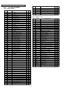
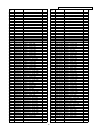
Pin
No.
Port Descriptions I/O
(V)
FM
(V)
AM
(V)
CD
(V)
64 KLIN.IN K-LINE data I 4.8 4.8 4.8
65 NC No connection - - - -
66 CDC.CLK CD CH clock I 4.8 4.8 4.8
67 BOSE BOSE Amp connection I 4.8 4.6 4.8
68 VDD +5V power supply - 48 4.8 4.8
69 VSS GND - 0 0 0
70 N.CNTR NAVI. control I 4.8 4.6 4.7
71 EXT.AMP.ON Ext Amp power control O 0 4.8 4.8
72 CAN.N.ERR CAN-BUS error I 4.8 0 4.8
73 CAN.EN CAN-BUS driver enable O 0 4.8 0
74 CAN.STB BUS data strobe O 0 1.9 0
75 CAN.RX CAN-BUS data I 4.8 2.2 2.2
76 CAN.TX CAN-BUS data O 4.8 0 2.4
77 CD.RST CD reset O 4.8 4.8 4.8
78 VDD +5V power supply - 4.8 4.8 4.8
79 VSS GND - 0 0 0
80 /RD Not used - - - -
81 /WR/WRL Not used - - - -
82 /READY Not used - - - -
83 ALE Not used - - - -
84 /EA (+5V pull-up) - 4.8 4.8 4.8
85 MUTE Mute O 4.8 4.8 4.8
86 KO.0 Key scan O 0 0.8 0.8
87 KO.1 Key scan O 0 0.8 0.7
88 KO.2 Key scan O 0 0.8 0.7
89 KO.3 Key scan O 0 0.8 0.7
90 KO.4 Key scan O 0 0.8 0.7
91 NC No connection - - - -
92 NC No connection - - - -
93 VDD +5V power supply - 4.8 4.8 4.8
94 VSS GND - 0 0 0
95 NC No connection - - - -
96 KI.0 Key data I 0 0 0
97 KO.5 Key scan O 0.7 0.8 0.7
98 NC No connection - - - -
99 NC No connection - - - -
100 AF.MUTE AF mute O 0 0 0
101 NC No connection - - - -
102 DSP RESET DSP reset O 0 0 0
103 M2 Not used - - - -
104 NC No connection - - - -
105 NC No connection - - - -
106 NC No connection - - - -
107 CD SW3 Audio mute I 0 0 0
108 KI.1 Key data I 0 0.6 0
109 KI.2 Key data I 1 0.7 0
110 KI.3 Key data I 1 0.7 0.7
111 VDD +5V power supply - 4.8 4.8 4.8
112 VSS GND - 0 0 0
113 KI.4 Key data I 1 0.7 0.7
114 NC No connection - - - -
115 CD.SIMO CD serial data O 0 0 0
116 CD STP/STA CD start/stop O 0 0 4.8
117 CD.SOMI CD serial data I 0 4.8 4.3
118 CD.SCKM CD data shift clock O 4.8 4.8 4.8
119 CD.ON CD power control O 4.8 4.8 4.8
120 NC No connection - - - -
121 VDD +5V power supply - 4.8 4.8 4.8
122 VSS GND - 0 0 0
123 XTAL2 Crystal oscillator - 2.2 2.2 2.2
124 XTAL1 Crystal osillator - 2.1 2.1 2.1
125 VSS GND - 0 0 0
126 XTAL3 Crystal oscillator - 1.2 1.2 1.2
127 XTAL4 Crystal oscillator - 2 2 2
128 /RSTIN Reset input I 4.7 4.7 4.7
Note : Voltage measuerments are with respect to ground, with
a voltmeter (internal resistance : 10M ohms).
8 TERMINALS DESCRIPTION
9
AUDI / CQ-JA1070L / CQ-JA1071L / CQ-JA1072L / CQ-JA1073L / CQ-JA1074L