


1998 Sep 23 10
Philips Semiconductors Product specification
4 × 25 W BTL quad car radio power
amplifier
TDA8567Q
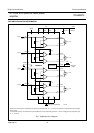
TEST AND APPLICATION INFORMATION
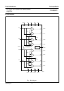
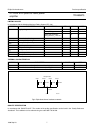
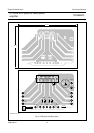
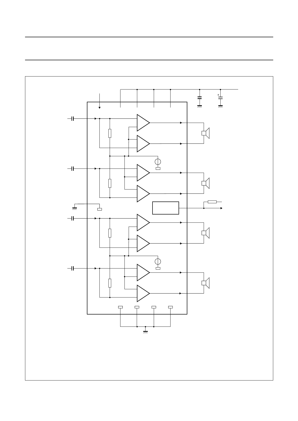
Fig.7 Application circuit diagram.
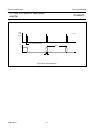
Special care must be taken in the PCB-layout to separate pin 9 from the pins 10, 11 13 and 14 to minimize the crosstalk between the clip output
and the inputs.
To avoid switch-on plops, it is advised to keep the amplifier in the mute mode during a period of ≥ 150 ms (charging the input capacitors at pin
10, 11, 13 and 14).
handbook, full pagewidth
MGG158
OUT1+
R
L
= 4 Ω
OUT1−
+
−
+
−
V
ref
2
IN1
input 1
IN2
input 2
4
15
10
MODE
2200 µF100 nF
23
+14.4 V
1681
V
P1
V
P2
V
P3
V
P4
V
P
30 kΩ
OUT2+
R
L
= 4 Ω
OUT2−
+
−
+
−
7
5
11
30 kΩ
470 nF
470 nF
470 nF
470 nF
211863
PGND1 PGND2 PGND3 PGND4
power ground (substrate)
OUT3+
R
L
= 4 Ω
OUT3−
+
−
+
−
V
ref
17
IN3
SGND
TDA8567Q
input 3
IN4
input 4
19
13
12
30 kΩ
OUT4+
R
L
= 4 Ω
OUT4−
+
−
+
−
22
20
14
30 kΩ
10 kΩ
V
DIAG
+V
P
DIAGNOSTIC
diagnostic
output
9