


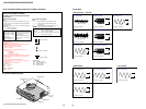
2020
CDX-GT50W/GT500/GT500EE/GT550
CDX-GT50W/GT500/GT500EE/GT550
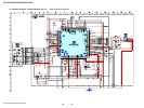
• NOTE FOR PRINTED WIRING BOARDS AND SCHEMATIC DIAGRAMS
THIS NOTE IS COMMON FOR PRINTED WIRING
BOARDS AND SCHEMATIC DIAGRAMS.
(In addition to this, the necessary note is printed
in each block.)
For schematic diagrams.
Note:
• All capacitors are in µF unless otherwise noted. (p: pF)
50 WV or less are not indicated except for electrolytics
and tantalums.
• All resistors are in Ω and
1
/
4
W or less unless otherwise
specified.
•
f
: internal component.
• C : panel designation.
For printed wiring boards.
Note:
• X : parts extracted from the component side.
• Y : parts extracted from the conductor side.
•
a
: Through hole.
• : Pattern from the side which enables seeing.
(The other layers' patterns are not indicated.)
• A : B+ Line.
• B : B– Line.
• H : adjustment for repair.
•Voltages and waveforms are dc with respect to ground
under no-signal (detuned) conditions.
• CD mechanism (1/2) and (2/2) sections
no mark : CD PLAY
• Main (1/3), (2/3), (3/3), Sub and Display sections
no mark : FM
(): AM/MW/LW
<>: CD PLAY
∗ : Impossible to measure
•Voltages are taken with a VOM (Input impedance 10 MΩ).
Voltage variations may be noted due to normal produc-
tion tolerances.
•Waveforms are taken with a oscilloscope.
Voltage variations may be noted due to normal produc-
tion tolerances.
• Circled numbers refer to waveforms.
• Signal path.
J : CD PLAY
F : FM
f : AM/MW/LW
L : AUX
Caution:
Pattern face side: Parts on the pattern face side seen from the
(Side B) pattern face are indicated.
Parts face side: Parts on the parts face side seen from the
(Side A) parts face are indicated.
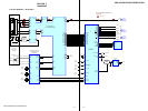
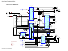
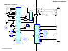
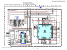
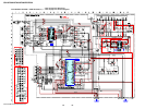
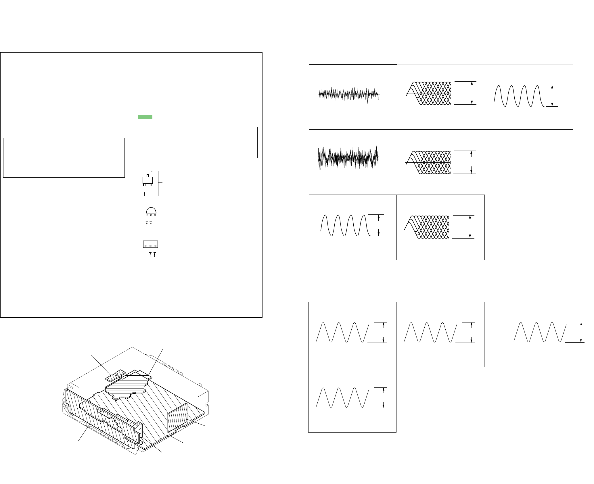
• WAVEFORMS
— SERVO BOARD — (CD PLAY)
— MAIN BOARD —
1 IC2 5 (FEI)
Approx.
1Vp-p
0 V
0.6 Vp-p
16.9344 MHz
Approx. 100 mVp-p
50 mV/DIV, 5 msec/DIV
0.5 V/DIV, 0.5
µ
sec/DIV
2 IC2 6 (TEI)
200 mV/DIV, 5 msec/DIV
6 IC2 oh (FPI2),
0.5 V/DIV, 0.5
µ
sec/DIV
Approx. 400 mVp-p
3 IC2 wd (XI)
0.2 V/DIV, 0.2
µ
sec/DIV
7 IC3 ia (X1)
0.5 V/DIV, 0.2
µ
sec/DIV
1.1 Vp-p
12 MHz
4 IC2 ia (RFI)
0.5 V/DIV, 0.5
µ
sec/DIV
5 IC2 of (FNI2),
og (FNI1)
1.5 Vp-p
oj (FPI1)
1.5 Vp-p
0 V
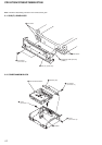
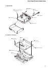
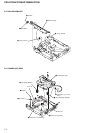
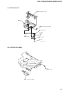
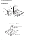
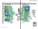
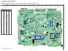
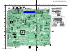
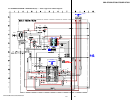
3-4. CIRCUIT BOARDS LOCATION
1.2 Vp-p
8.664 MHz
1 IC350 0 (XTO)
0.5 V/DIV, 0.1
µ
sec/DIV
0.8 Vp-p
32.768 kHz
2 IC711 i; (XOUT)
0.5 V/DIV, 0.1
µ
sec/DIV
0.9 Vp-p
18.432 MHz
3 IC711 is (OSCOUT)
0.5 V/DIV, 0.1
µ
sec/DIV
0.9 Vp-p
5 MHz
1 IC901 qs (X1)
0.5 V/DIV, 0.1
µ
sec/DIV
— KEY BOARD —
MAIN board
SUB board
SENSOR board
SERVO board
KEY board
tuner uni
t
(TU300)
Q
C
These are omitted
EB
E
These are omitted
CB
C
These are omitted
BE
• Abbreviation
CND : Canadian model
EE : East European model
MX : Mexican model
CH : Chinese model
Note:
The components identi-
fied by mark 0 or dotted
line with mark 0 are criti-
cal for safety.
Replace only with part
number specified.
Note:
Les composants identifiés par
une marque 0 sont critiques
pour la sécurité.
Ne les remplacer que par une
piéce portant le numéro
spécifié.