iv
Intel
®
440GX AGPset Design Guide
2.6 Validation ....................................................................................................2-15
2.6.1 Flight Time Measurement ..............................................................2-15
2.6.2 Signal Quality Measurement..........................................................2-16
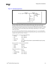
2.7 Timing Analysis...........................................................................................2-17
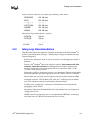
2.8 AGP Layout and Routing Guidelines ..........................................................2-19
2.8.1 AGP Connector (“Up Option) Layout Guidelines ...........................2-19
2.8.2 On-board AGP Compliant Device (“Down” Option)
Layout Guidelines ..........................................................................2-20
2.9 82443GX Memory Subsystem Layout and Routing Guidelines..................2-22
2.9.1 100 MHz 82443GX Memory Array Considerations........................2-22
2.9.1.1 Matching the Reference Planes ...................................2-23
2.9.1.2 Adding Additional Decoupling Capacitor ......................2-23
2.9.1.3 Trace Width vs. Trace Spacing ....................................2-24
2.9.2 Memory Layout & Routing Guidelines ...........................................2-24
2.9.3 4 DIMM Routing Guidelines [NO FET]...........................................2-30
2.9.4 PCI Bus Routing Guidelines ..........................................................2-30
2.9.5 Decoupling Guidelines: Intel
®
440GX AGPset Platform ...............2-31
2.9.6 Intel
®
440GX AGPset Clock Layout Recommendations................2-32
2.9.6.1 Clock Routing Spacing .................................................2-32
2.9.6.2 System Bus Clock Layout.............................................2-32
2.9.6.3 PCI Clock Layout..........................................................2-33
2.9.6.4 SDRAM Clock Layout...................................................2-33
2.9.6.5 AGP Clock Layout ........................................................2-34
3 Design Checklist ........................................................................................................3-1
3.1 Overview.......................................................................................................3-1
3.2 Pull-up and Pull-down Resistor Values.........................................................3-1
3.3 Intel
®
Pentium
®
II Processor Checklist.........................................................3-2
3.3.1 Intel
®
Pentium
®
II Processor ...........................................................3-2
3.3.2 Intel
®
Pentium
®
II Processor Clocks................................................3-5
3.3.3 Intel
®
Pentium
®
II Processor Signals...............................................3-5
3.3.4 Uni-Processor (UP) Slot 1 Checklist................................................3-7
3.3.5 Dual-Processor (DP) Slot 1 Checklist..............................................3-7
3.3.6 Slot 1 Decoupling Capacitors ..........................................................3-7
3.3.7 Voltage Regulator Module, VRM 8.2 ...............................................3-7
3.4 Intel
®
440GX AGPset Clocks........................................................................3-8
3.4.1 CK100 - 100 MHz Clock Synthesizer...............................................3-8
3.4.2 CKBF - SDRAM 1 to 18 Clock Buffer...............................................3-9
3.4.3 GCKE and DCLKWR Connection....................................................3-9
3.5 82443GX Host Bridge.................................................................................3-10
3.5.1 82443GX Interface.........................................................................3-10
3.5.2 82443GX GTL+ Bus Interface .......................................................3-12
3.5.3 82443GX PCI Interface..................................................................3-12
3.5.4 82443GX AGP Interface ................................................................3-13
3.6 Intel
®
440GX AGPset Memory Interface ....................................................3-14
3.6.1 SDRAM Connections.....................................................................3-14
3.6.2 DIMM Solution With FET Switches................................................3-15
3.6.3 Registered SDRAM .......................................................................3-15