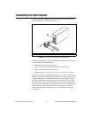
© National Instruments Corporation 11 SCC-AI Series Isolated Analog Input Modules
Scaling Voltage Measurements
If you configured the SCC-AIXX using MAX and you are using NI-DAQ,
the voltage reading you get from the E Series DAQ device accounts for the
voltage scaling effect of the SCC-AIXX. Otherwise, since the voltage
measurement from the E Series DAQ device is scaled by the gain given in
Table 1-1, you must divide the voltage reading returned by the E Series
DAQ device by this gain to get the correct input voltage.
Specifications
These ratings are typical at 25 °C unless otherwise stated.
Input Characteristics
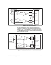
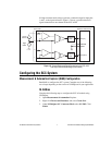
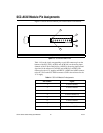
Number of input channels...................... 2 NRSE
Isolation.................................................. Bank isolation (isolation
per module)
1
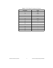
Input/output signal range, gain,
and bandwidth........................................ Refer to Table 1-1
Input impedance
SCC-AI01, SCC-AI02 .................... 1 MΩ
All others......................................... 100 MΩ
Gain error............................................... 4.5% max (trimmable to zero)
Gain stability.......................................... 150 PPM/°C
Offset error............................................. 40 mV max (RTI
2
)
Offset stability........................................ 225 µV/°C
Nonlinearity ........................................... 0.0128% typ
0.0260% max
Common-mode rejection ratio ............... 100 dB typical at 60 Hz
Output slew rate,
dependent on BW (filtering) .................. 0.8 V/µs max
1
The SCC-AIXX does not provide isolation between the two channels of the module. For more information on this topic,
refer to the Connecting the Input Signals section.
2
This specification is calculated relative to the input range of the module.