


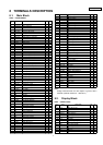
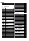
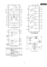

61 DO Key data output O 4.1
62 CE LCD driver chip enable I 0
63 CL Shift clock for LCD data I 0
64 DI LCD data input I 0
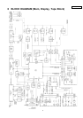
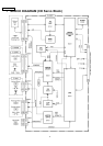
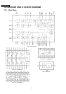
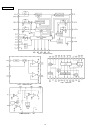
8.3. CD Servo Block
IC201 : MN662783RPW
Pin
No.
Port Description I/O (V)
1 VDD +5V power supply - 5.0
2 D0 D-RAM data I/O 2.3
3 D1 D-RAM data I/O 1.8
4 /WE D-RAM data write O 4.9
5 /RAS D-RAM row address strobe O 3.4
6 D2 D-RAM data I/O 0.8
7 D3 D-RAM data I/O 0
8 /CAS0 D-RAM columun address strobe O 3.9
9 /CAS1 D-RAM columun address strobe O 0
10 A8 D-RAM address O 0.6
11 A7 D-RAM address O 1.1
12 A6 D-RAM address O 0.7
13 A5 D-RAM address O 0
14 A4 D-RAM address O 1.1
15 A9 D-RAM address O 0.4
16 A0 D-RAM address O 1.0
17 A1 D-RAM address O 1.0
18 A2 D-RAM address O 1.0
19 A3 D-RAM address O 0
20 VSS2 Ground - 0
21 VDD2 +5V power supply - 5.0
22,23 - Not used - -
24 TVD Traverse motor control O 2.5
25 PC Not used - -
26 ECS Spindle motor control O 2.4
27 TRD Tracking coil drive O 2.5
28 FOD Focus coil drive O 2.4
29 FBAL Focus balance O 1.9
30 TBAL Tracking balance O 3.0
31 VREF Reference voltage I 2.5
32 FE Focus error I 2.5
33 TE Tracking error I 2.5
34 RFENV RF envelope I 2.5
35 OFT Off track signal I 0
36 /RFDET RF detecting signal I 0
37 BDO Drop-out signal I 0
38 LDON Laser on signal O 4.5
39 ARF RF signal I 2.5
40 IREF Reference current input I 1.2
41 DRF Biase for DSL I 2.4
42 DSLF Loop filter for DSL I/O 2.5
43 SDLF2 Loop filter for DSL I/O 2.2
44 PLLF Loop filter for PLL I/O 1.4
45 VCOF Not used - -
46 AVDD2 +5V power supply - 5.0
47 AVSS2 Ground - 0
48 OUTL L channel output O 2.3
49 AVSS1 Ground - 0
50 OUTR R channel output O 2.3
51 AVDD1 +5V power supply - 4.7
52-54 - (Connecting to ground) - 0
55 FLAG Flag output O 0
56 FCLK Frame clock O 0
57-59 - Not used - -
60 TX Not used - -
61 MCLK Clock for I/F command I 1.0
62 MDATA Data for I/F command I 3.1
63 MLD I/F command load I 5.0
64 BLKCK Subcode block clock O 0
65 SQCK Ext. clock for sub code-Q I 5.0
66 SUBQ Code for sub. code-Q O 3.8
67 DMUTE Mute input I 0
68 STAT Status signal O 5.0
69 /RST Reset input I 5.0
70 CSEL (Connecting to ground) - 0
71 PMCK PM clock O 2.5
72 SMCK SM clock O 2.5
73 SUBC Serial data of sub code O 0
74 SBCK Shift clock for SUBC I 0.6
75 /CLDCK Not used - -
76 /TEST (Connecting to VDD) - 5.0
77 X1 Crystal oscillator - 0.4
78 X2 Crystal oscillator - 3.2
79 VDD1 +5V power supply - 5.0
80 VSS1 Ground - 0
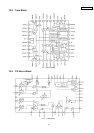
IC301 : MN1873260AB4
Pin
No.
Port Description I/O (V)
1 VDD +5V power supply - 5.0
2 OSC2 Crystal oscillator - 2.2
3 OSC1 Crystal oscillator - 2.1
4 VSS Ground - 0
5 XI (Connecting to ground) - 0
6 XO Not used - -
7 CM (Connecting to ground) - 0
8 VREFH Reference voltage I 5.0
9 SW13 Shuter SW I 4.9
10 SW12 Horizontal origin I 4.9
11 SW11 Clump SW I 0
12 SW10 Play SW I 0
13 SW4 Shuter SW I 4.9
14 SW3 Tray origin SW I 0
15 SW2 Inner SW I 4.8
16 SW1 Outer SW I 4.9
17 VREFL Reference voltage I 0
18 /RESET Reset input I 4.9
19 - (Ground pull-down) - 0
20 SCKM Clock for serial data I 5.0
21 SIM CD changer serial data I 1.3
22 SOM CD changer serial data O 4.3
23 SQCK Ext. clock for sub. code-Q O 5.0
24 SUBQ Code for sub. code-Q I 1.6
25 - Not used - 5.0
26 - (Ground pull-down) - 0
27 CD.ON CD changer start/stop I 5.0
28 - Not used - 5.0
29 BLKCK Sub. code block clock I 0
30 P.ON Not used - 5.0
31 MUTE Mute output O 5.0
32 - (Ground pull-down) - 0
33 SENS Servo status O 0
34 CLVS Servo status O 5.0
35 FLOCK Focus servo lock O 0.2
36 TLOCK Tracking servo lock O 0
37 VMI Horizontal motor control O 2.5
38 HMI Vertical motor control O 0
39 HVMUTE H/V motor mute O 0
40-42 - (Ground pull-down) - 0
43 SW9 Disc-in (B) SW I 0
44 SW8 Disc-in (L) SW I 0
45 SW7 Disc-in (F) SW I 0
46 SW6 Disc push SW I 0
8
HONDA / CQ-EH8160AK