


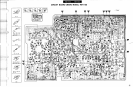
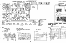

[Q]
-~---;:."
eI
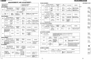
Vss I Power supply terminal (5V).
28
~
.
.:=:::.--
21-27
I
a1-g1
1 7-segment drive output terminal.
This output terminal for enabling display of the
digit corresponding to units of 100kHz
in
the FM
mode and the digit corresponding to units of 1
kHz in the
AM
mode.
Pin No.
ISymbol1
Description
04
02
01
Description
OaI8-------"[
CK,
CK>
A data signal is composed of 16bits. Eleven bits
are assigned for frequency dataand the remain-
ing 5 bits are assigned for the reception bands.
Receiving frequency data input control timing
input terminal.
Each time a data signal is sent, a timing signal is
concurrently sent from pins 20 and
21
of IC7 to
this terminal, to read the data signal.
Two lines
(CK-1
and CK-2) are used for timing
the data signal reading. They have the following
timing relationship with the data signal.
a-'OO~see
01
02
D4
DB
016 032064DI28D2S6D51201024LWFMJFMUAM9AM10
Dala
8 Flequency
DaUl
".--------11----
I/O I Segment drive output terminal.
This output terminal enables display of the digit
corresponding to units
of
100 MHz in the FM
mode and the digit corresponding to units of
1000 kH
in
the AM mode.
Data
I Receiving frequency data input terminal.
A datasignal containing the receiving frequency
and band is sent to this terminal from pin 22 of
IC7 (RVITC9137P) each time the receiving
frequency is changed.
CK1,
CK2
2
5
3,4
14 I GND I Ground terminal.
1
I UD I Output condition switching input terminal.
This terminal sets the display output mode
(LED, FL, or LCD).
LED Make this terminal
"H"
level.
FL Make this terminal
"L"
level.
LCD Apply AC voltage to this terminal.
6-12
I
a3-g31
7-segment drive output terminal.
This output terminal enables display
of
the'digit
corresponding to units of 10 MHz
in
the
FM
mode and the digitcorresponding to units of 100
kHz in the
AM
mode.
Pin No. ISymbol
13.15-201
a2-g2
17-segment drive output terminal.
This output terminal enables display of the digit
corresponding to units
of
1 MHz
in
the
FM
mode
and the digit corresponding to units of
10kHz
in
the
AM
mode.
3)
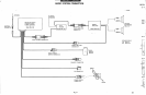
Explanation of each terminal
[[]
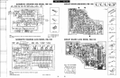
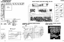
RM-1100 RM-1100
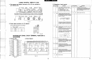
Fig.
24
I a2 I
I_I
19
2
l
d2
IC403
'
0
c2
1
___
1-
"-
__
Pin 20 (a2)
1'tlliIWlJ
Pin 19 (b2)
~
I
Pin 18 (c2)
~~
Pin 17 (d2)
~
Pin 16 (e2)
l..J-Lri
Pin 15 (f2)
J-u-1
I I
Pin 13 (92) 1---uL!
COM 2
:~
r :
Fig.
22-1
Fig.
22
2)
Block Diagram
~
$
~~
~
Vcc
01
bl
cl
DATA
dl
CK I
el
CK2
f I
gl
02
b2
c2
d2
e2
f2
Al.M
F M
F
LIQUID CRYSTAL DISPLAY (LCD)
A
il-I::EI::EI~IOI~
8<n!L«<n-l-
:E
o
u
RVITD6301AP (IC403): EACH TERMINAL FUNCTION &
WAVEFORM
Phase of segment
No. signal vs. common
Segments of LCD
signal
1 Oposite
ON
2 Same
OFF
Fig.
22-1
indicates the timing chart of LCD operation.
2)
Output signal waveforms of
LCD
segment
1)
The common and segment terminals of the
LCD
are connected
in
the following way:
L/D
Data
CKI
CK2
I/O
g3
f3
e3
d3
c3
b3
03
g2
GND
I
114
Fig.
23
1)
Terminal View
."
$
j