


2004 May 05 10
Philips Semiconductors Preliminary specification
Power stage 2 x 10 or 1 x 20 W class-D
audio amplifier
TDA8928J
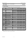
14 SWITCHING CHARACTERISTICS
V
P
= ±12.5 V; T
amb
=25°C; measured in Fig.4; unless otherwise specified.
SYMBOL PARAMETER CONDITIONS MIN. TYP. MAX. UNIT
PWM outputs (pins OUT1 and OUT2); see Fig.3
t
r
rise time − 30 − ns
t
f
fall time − 30 − ns
t
blank
blanking time − 70 − ns
t
PD
propagation delay from pin SW1 (SW2) to
pin OUT1 (OUT2)
− 200 − ns
t
W(min)
minimum pulse width − 220 270 ns
R
ds(on)
on-resistance of the output
transistors
− 0.2 0.4 Ω
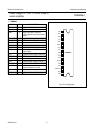
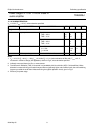
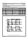
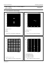
handbook, full pagewidth
MGW145
PWM
output
(V)
V
DD
V
SS
0 V
t
blank
t
f
t
r
1/f
osc
100 ns
V
STAB
V
SS
V
SW
(V)
t
PD
V
STAB
V
SS
V
REL
(V)
Fig.3 Timing diagram PWM output, switch and release signals.