


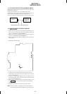

– 11 –
4-1. IC PIN DESCRIPTIONS
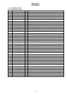
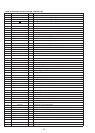
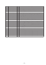
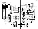
• IC100 CXA2523AR (RF AMP)
Pin No. Pin Name I/O Pin Description
1 I I I-V converted RF signal input (I) from detector of optical pick-up.
2 J I I-V converted RF signal input (J) from detector of optical pick-up.
3 VC O Center voltage (+1.65 V) generation output
4 – 9 A – F I Signal input (A to F) from detector of optical pick-up.
10 PD I Quantity monitor input of light from laser diode of optical pick-up.
11 APC O Laser amplifier output to automatic power control circuit.
12 APCREF I Reference voltage input for laser power setting.
13 GND — GND
14 TEMPI I Temperature sensor connecting pin (Not used in this set.)
15 TEMPR O Reference voltage output for temperature sensor. (Not used in this set.)
16 SWDT I Write data signal input from System controller (IC600).
17 SCLK I Serial clock signal input from System controller (IC600).
18 XLAT I Serial latch signal input from System controller (IC600).
19 XSTBY I Standby signal input (“L” : Standby) (Fixed at “H” in this set.)
20 FOCNT I Center frequency control voltage input of internal circuit filter (BPF22, BPF3T and EQ).
21 VREF O Reference voltage output (Not used in this set.)
22 EQADJ I Center frequency setting input of internal circuit filter (EQ).
23 3TADJ I Center frequency setting input of internal circuit filter (BPF3T).
24 VCC — Power supply pin (+3.3 V)
25 WBLADJ I Center frequency setting input of internal circuit filter (BPF22).
26 TE O Tracking error signal output to CXD2652AR (IC200).
27 CSLED I Connecting pin for low pass filter condenser of sled error signal.
28 SE O Sled error signal output to CXD2652AR (IC200).
29 ADFM O FM signal output of ADIP.
30 ADIN I FM signal input of ADIP by AC combination.
31 ADAGC I External condenser connecting pin for AGC of ADIP.
32 ADFG O ADIP double FM signal output (22.05 kHz ± 1 kHz) to CXD2652AR (IC200).
33 AUX O Support signal (I3 signal/temperature signal) output (Not used in this set.)
34 FE O Focus error signal output to CXD2652AR (IC200).
35 ABCD O Quantity signal output of light to CXD2652AR (IC200).
36 BOTM O Bottom hold signal output of quantity signal (RF/ABCD) of light to CXD2652AR (IC200).
37 PEAK O Peak hold signal output of quantity signal (RF/ABCD) of light to CXD2652AR (IC200).
38 RF O Playback EFM RF signal output to CXD2652AR (IC200).
39 RFAGC I External condenser connecting pin of AGC circuit for RF.
40 AGCI I RF signal input by AC combination.
41 COMPO O User comparator output pin (Not used in this set.)
42 COMPP I User comparator input pin (Fixed at “L” in this set.)
43 ADDC I External condenser connecting pin for low frequency interception of ADIP amplifier.
44 OPO O External condenser connect pin for lower cut of ADIP amplifier.
45 OPN I User operational amplifier inversion input pin (Fixed at “L” in this set.)
46 RFO O RF signal output
47 MORFI I RF signal input of MO by AC combination.
48 MORFO O RF signal output of MO.
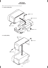
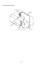
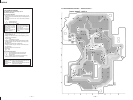
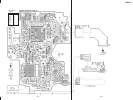
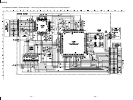
SECTION 4
DIAGRAMS