


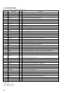
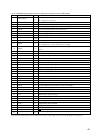
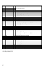
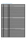
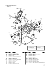

53
55 HLDA/ALE O Microprocessor mode output. (Not used.)
56 MNT2 (XBUSY) I In the state of executive command from the CXD2662R
57 VSS — Ground.
58 (MNT1) SHCK I Track jump signal input from the CXD2662R
59 VCC — Power supply. (+3.3V)
60 EEP-WP O EEP-ROM write protect signal output. L: write possibility
61 SDA I/O Data signal input/output pin with the EEP-ROM.
62 BUS CLK O Not used.
63 OE O Read signal output.
64 BHE CASH O Not used.
65 WE R/W O Write signal output.
66 SCL O Clock signal output to the EEP-ROM.
67 REFLECT-SW I Disk reflection rate detection input from the reflect detection switch. H: Disk with low reflection rate
68 PROTECT-SW I Recording-protection claw detection input from the protection detection switch. H: Protect
69 CS0 O Chip select signal output to the Flash ROM.
70 CS1 O Not used.
71 CS2 O Not used.
72 A20 O Not used.
73 A19 O Address bus signal output to Flash ROM.
74 VCC — Power supply. (+3.3V)
75 A18 O Address bus signal output to Flash ROM.
76 VSS — Ground
77 to 85 A17 to A9 O Address bus signal output to Flash ROM.
86 to 89 MODEL SEL 1 to 4 O Not used.
90 WP O Write protect signal to the Flash ROM.
91 VCC — Power supply. (+3.3V)
92 A8 O Address bus signal output to Flash ROM.
93 VCC — Power supply. (+3.3V)
94 to 101 A7 to A0 LB O Address bus signal output to Flash ROM.
102 to 113 D15 to D4 I/O Data bus signal input/output to the Flash ROM.
114 K.B-CLK-CTRL O Keyboard clock ON/OFF signal output. L: OFF H: ON
115 IIC BUSY O IIC cable connect check. L: Active
116 K.B-DATA O Keyboard data output.
117, 118 REC-VOL B, A O Not used.
119 to 122 D3 to D0 I/O Data bus signal input/output to the Flash ROM.
123, 124 JOG1, JOG0 I Jog dial pulse input from the rotary encoder.
125 LATCH(DA) O Not used.
126 REC O Mute signal output when Beep Rec.
127 NC O Not used.
128 CS(FL) O Chip select signal output to the display driver.
129 POWER(IIC) O Media commucator start-up check.
130 VSS — Ground.
131 STB O Strobe signal output to the power supply circuit. H: Power supply ON: L: standby
132 VCC — Power supply. (+3.3V)
133 IOP I Optical Pick-up voltage (current) detect signal input.
134 (A/D-6) I Model discrimination.
135 (A/D-5) I Model discrimination.
136 TIMER/BEEP SW I Timer mode select signal input.
137 to 139 KEY 3 to KEY 1 I Key input pin (A/D input)
140 AVSS — Ground. (Analog)
141 KEY0 I A/D reference voltage.
142 VREF — Power supply. (+3.3V)
143 AVCC — Power supply. (+3.3V)
144 NC I Not used.
FunctionPin NamePin No. I/O