


– 7 –
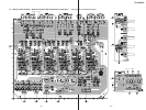
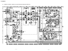
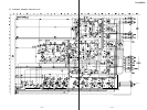
SECTION 4
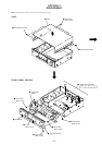
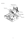
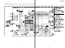
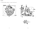
DIAGRAMS
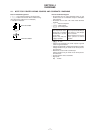
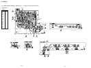
Note on Printed Wiring Board:
• X : parts extracted from the component side.
• b : Pattern from the side which enables seeing.
(The other layers' patterns are not indicated.)
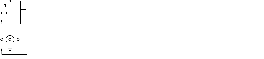
• Indication of transistor.
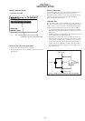
4-1. NOTE FOR PRINTED WIRING BOARDS AND SCHEMATIC DIAGRAMS
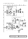
B
These are omitted.
CE
Q
C
B
These are omitted.
E
Q
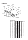
Note on Schematic Diagram:
• All capacitors are in µF unless otherwise noted. pF: µµF
50 WV or less are not indicated except for electrolytics
and tantalums.
• All resistors are in Ω and
1
/
4
W or less unless otherwise
specified.
•
¢
: internal component.
• 5 : fusible resistor.
• C : panel designation.
• U : B+ Line.
• V : B– Line.
• Voltages and waveforms are dc with respect to ground
under no-signal conditions.
• Voltages are taken with a VOM (Input impedance 10 MΩ).
Voltage variations may be noted due to normal produc-
tion tolerances.
• Waveforms are taken with a oscilloscope.
Voltage variations may be noted due to normal produc-
tion tolerances.
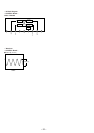
• Circled numbers refer to waveforms.
• Signal path.
F : AUDIO
Note:
The components identi-
fied by mark ! or dotted
line with mark ! are criti-
cal for safety.
Replace only with part
number specified.
Note:
Les composants identifiés par
une marque ! sont critiques
pour la sécurité.
Ne les remplacer que par une
piéce portant le numéro
spécifié.