


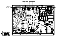
The circuitry around SK201A and IC200 is to receive and
demodulate remote control commands sent in via the rear
panel jack socket. This is for multi-room applications. L200
and C200 form a parallel resonant circuit at approximately
37kHz. The output from this bandpass filter is passed into
IC200A where it is ‘chopped’ and fed to IC200B to provide
the output signal.
SK201B is a 13VDC signal trigger output which is active
whenever the amplifier is powered up. R218 and DZ207 /
C223 provide a reference voltage which is buffered by
TR200. TR201 and R217 act as a current limit and prevent
damage due to a short circuit on the output of SK201B. The
maximum current is approximately 65mA.
TR203 and TR202 are a complementary Darlington pair
which turn on mains relay RLY200 when activated by a
signal from the microprocessor.
TR204 and its associated components are to detect whenever
AC mains is present at the IEC socket. This is to notify the
microprocessor if the user has unplugged the mains cord, so
that it can take the necessary action (muting all the outputs
and switching off the mains relay). The reservoir capacitors
should last at least 4 mains cycles which gives the
microprocessor plenty of time for a controlled shutdown.
TR204 forms a monostable circuit. Each cycle of AC turns on
TR204 via R211. TR204 then ‘shunts’ C229 ensuring that it
is kept at a low potential. If more than one mains cycle is
missing, then R219 charges up C229 sufficiently to trigger
Schmitt inverter IC202E thus passing on a logic signal to the
microprocessor. The use of a Schmitt inverter for IC202 is to
ensure that the micro receives ‘clean’ logic levels - the
hysteresis voltage (about 0.5V) is sufficient to prevent circuit
noise from producing a string of ‘ghost’ signals when
analogue levels are near the threshold point.
TH200 is a positive tempco thermistor placed adjacent to the
heatsink on which the output transistors are mounted. When
the temperature of the thermistor exceeds 90 degrees Celsius
the thermistor goes to a high impedance and so the input to
IC202F goes low. This triggers a HIGH output to the micro
indicating thermal overload.
The VI protection signals from the left and right channels
pass into IC202A and IC202B respectively, to be ‘cleaned
up’ via the Schmitt trigger. They are then NOR’d using
TR205 which sends a HIGH signal to the micro in the event
of either channel suffering a short circuit or current overload.
Exactly the same approach is used for the DC fault lines
using IC202C and IC202D.
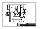
L882 Circuit Sheet 3
This is the main audio power amplifier circuit. The amplifier
is a class B design, which uses SAP ‘audio’ transistors in a
symmetrical current feedback configuration. Input and
feedback paths are DC coupled and there is an active
integrating servo to remove DC offsets from the output.
The basic principle of operation is follows:
The input signal is amplified by a factor of 2 in IC300A. This
drives a 44˜ impedance to ground causing the supply pin
currents to change with the signal level. These changing
supply pin currents are then ‘reflected’ by a pair of
complementary Wilson mirrors and passed on to a series of
buffer transistors before being connected to the load. The
‘feedback current’ flows back from the output terminal via
R331 and R332 and attempts to provide the current necessary
to allow IC300A to swing its output without drawing
excessive current from its supply pins, thus making the
change in supply current very small indeed. This is why the
term ‘current feedback’ is used - it is the current flowing in
the feedback resistors that sets the overall gain of the
amplifier.
IC300B acts as an inverting integrator and its purpose is to
remove DC from the loudspeaker output. Any positive DC
offset will cause the output of IC300B to go negative, thus
increasing the current in its negative supply pin and
pulling the output voltage back towards zero. R330 and
C317 set the time constant of this integrator (0.47 seconds)
so that audio frequency components are ignored and only
DC and subsonic frequencies are removed.
The input to the amplifier is limited to ±5.4V via back-to-
back zener diodes DZ302 and DZ303. This is to prevent
the user from grossly overdriving the input to the amplifier
and possibly causing damage. The diodes appear before
series resistor R324 so that their variable capacitance does
not introduce high frequency harmonic distortion.
R324, R327 and C316 act as an input filter - this is a first
order low pass filter with a corner frequency of around
340kHz to prevent RF signals from being injected into the
front end of the amplifier. The corner frequency was
chosen such that the phase shift introduced is less than 5˜
at 20kHz (considered by the AES to be the minimum
perceptible relative amount by the human ear). The input
impedance of the amplifier is 23kW at DC, falling to
around 14kW at 20kHz.
Operational amplifier IC300A is acting as a non-inverting
gain of 2, driving the input signal into a 44W impedance to
ground via R322 and R337. Its output voltage will be an
accurate amplification of its input voltage (i.e. the signal
on pin 1 should look identical to that on pin 3 but at twice
the amplitude). The op-amp is used in a slightly unusual
configuration here, in that its power supply pins are used
as a (current) output, and its output pin is used as a
(current) feedback.
Transistors TR311 and TR303 supply the ±15V rails to the
op-amp, and act as cascades to pass its supply pin currents
through to the current mirrors, which sit at a potential too
high for the op-amp to be connected directly.
TR300, TR301 and TR321 form a PNP Wilson current
mirror, which reflects the current sunk by the positive
supply pin of IC300. Likewise TR314, TR315 and TR320
form an NPN Wilson current mirror, which reflects the
current sourced by the negative supply pin of IC300.
R315 thru R318 provide emitter degeneration of
approximately 300mV for the current mirrors (as they pass
about 3mA DC in quiescent conditions), to ensure accurate
operation independent of the small variations between the
transistors in the current mirrors. They also ensure that the
current passing down the next stage is reasonably constant
as the internal temperature of the amplifier changes,
swamping out small thermal variations in the
VBE
of the
mirror transistors.
R319 and R320 slightly decouple the rails to the current
mirrors from the main power rails of the amplifier, to
allow the bootstrap circuit to operate. The bootstrap
consists of C302 and C306 with metal film power resistors
R352 and R353. The bootstrap is provided to allow the
power supply rails of the current mirrors to go up and
down slightly with the output signal into the loudspeaker.
This enables the driver stage to fully saturate the output
transistors and thus give the greatest power output and best
thermal efficiency for any given power rail voltage. The
voltage on the ‘inside’ end of R319 and R320 will vary by
about 12 volts peak to peak at full output power, rising
above the main power rails during signal peaks.