


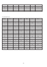
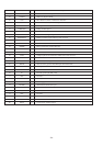
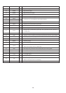
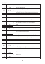
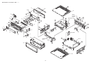

Pin No. Pin Name I/O Description
39 RVSS - Right channel ground. (Must be connected to 0V.)
40 RCHO O Right channel output.
41 RVDD - Right channe power supply.
42 MUTER/CONT8 O Right channel mute output./ General purpose input/ output.
43 XVDD - Crystal oscillator power supply.
44 XOUT O
Connections for a 16.9344 MHz crystal oscillator element.
45 XIN I
46 XVSS - Crystal oscillator ground. (Must be connected to 0V.)
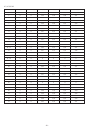
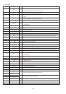
47 SBSY O Subcode clock synchronization signal output.
48 EFLG O C1, C2, sigle an double error correction monitor.
49 PW O Subcode P, Q, R, S, T, U and W output.
50 SFSY O
Subcode frame synchronization signal output. This signal falls when the subcode are
in standby stase.
51 SBCK I Subcode readout clock input. This is a Schmitt input.
52 FSX O Output pin for the 7.35 kHZ synchronization signal divided from the crystal oscillator.
53 WRQ O Subcode Q output standby output.
54 RWC I Read/write control input. This is a Schmitt input.
55 SQOUT O Subcode Q output.
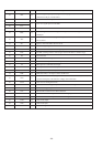
56 COIN I Command input pin from control microprocessor.
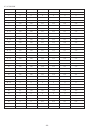
57 CQCK I
Input for both the command input acquisition clock and the SQOUT pin subcode
readout clock input pin. This is Schmitt input.
58 RES I Reset input. This pin must be set low briefly after power is first applied.
59 TST11 O Test output. Leave open. (Normally output a low level.)
60 16M O 16.9344 MHz output.
61 4.2M O 4.2336 MHz output.
62 TEST5 I Test input. A pull-down resistor is built-in. (Must be connected to 0V.)
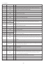
63 CS I
Chip seledt input. A pull-down resistor is built-in.
(Must be connected to 0V if not controlled.)
64 TEST1 I Test input. No pull-down resistor. (Must be connected to 0V.)
- 28 -