


2002 Mar 05 5
Philips Semiconductors Product specification
4 × 40 W BTL quad car radio power
amplifier
TDA8571J
FUNCTIONAL DESCRIPTION
The TDA8571Jcontains fouridentical amplifierswhich can
be used for bridge applications. The gain of each amplifier
is fixed at 34 dB.
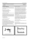
Mode select switch (pin MODE)
• Standby: low supply current (<100 µA)
• Mute: input signal suppressed
• Operating: normal on condition.
Since this pin has a low input current (<80 µA), a low cost
supply switch can be applied.
To avoid switch-onplops, it isadvised to keepthe amplifier
in the mute mode during ≥150 ms (charging of the input
capacitors at pins IN1, IN2, IN3 and IN4. When switching
from standby to mute, the slope should be at least 18 V/s.
This can be realized by:
• Microprocessor control
• External timing circuit (see Fig.3).
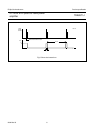
Diagnostic output (pin V
DIAG
)
D
YNAMIC DISTORTION DETECTOR (DDD)
At the onset of clipping of one or more output stages, the
dynamic distortion detector becomes active and pin V
DIAG
goes LOW. This information can be used to drive a sound
processor or DC volume control to attenuate the input
signal and so limit the distortion. The output level of
pin V
DIAG
is independent of the number of channels that
are clipping (see Fig.4).
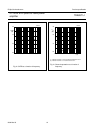
S
HORT-CIRCUIT DIAGNOSTIC
When a short-circuit occurs at one or more outputs to
ground or to the supply voltage, the output stages are
switched off until the short-circuit is removed and the
device is switched on again, with a delay of approximately
10 ms after removal of the short-circuit. During this
short-circuit condition, pin V
DIAG
is continuously LOW.
When a short-circuit occursacross the load of oneor more
channels, the output stages are switched off during
approximately 10 ms. After that time it is checked during
approximately 50 µs to determine whether the short-circuit
is still present. Due to this duty cycle of 50 µs/10 ms the
average current consumption during this short-circuit
condition is very low.
During this short-circuit condition, pin V
DIAG
is LOW for
10 ms and HIGH for 50 µs (see Fig.5). The protection
circuits of all channels are coupled. This means that if a
short-circuit condition occurs in one of the channels, all
channels are switched off. Consequently, the power
dissipation in any short-circuit condition is very low.
TEMPERATURE PRE-WARNING
When the virtual junction temperature T
vj
reaches 145 °C,
pin V
DIAG
goes LOW.
OPEN-COLLECTOR OUTPUTS
The diagnostic pin has an open-collector output, so more
devices can be tied together. An external pull-up resistor is
needed.
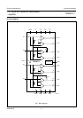
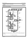
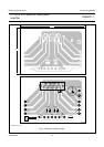
Fig.3 Mode select switch circuitry.
handbook, halfpage
+V
P
MODE
MGD959
BZX79C/3.9V
10 kΩ
47 µF
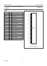
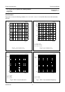
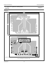
Fig.4 Distortion detector waveform.
handbook, halfpage
V
9
0
V
P
V
o
0
t
MGG155