


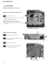
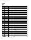
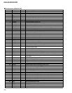
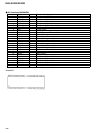
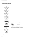
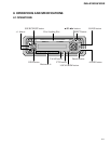
56
DEH-2130R,2100R
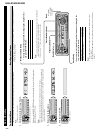
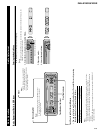
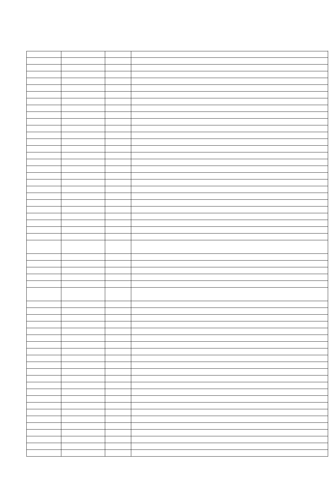
- Pin Functions (UPD63711GC)
Pin No. Pin Name I/O Function and Operation
1 D.GND Logic circuit GND
2 RFOK O RFOK signal output
3 rst I Reset signal input
4 A0 I Command/parameter identification signal input
5 stb I Data strobe signal input
6 sck I Clock signal input for serial data input/output
7 SO O Serial data and status signal output
8 SI I Serial data input
9 xtalen I Crystal oscillation control pin
10 D.VDD Positive power supply terminal to logic circuit
11 DA.VDD Positive power supply terminal to D/A converter
12 R_OUT O Right channel audio output signal
13 DA.GND D/A converter GND
14 REGC I The outside putting capacitor connection pin for SCF regulator
15 DA.GND D/A converter GND
16 L_OUT O Left channel audio output signal
17 DA.VDD Positive power supply terminal to D/A converter
18 R+ O Right channel audio data output
19 R- O Right channel audio data output
20 L- O Left channel audio data output
21 L+ O Left channel audio data output
22 X.VDD Positive power supply terminal to crystal oscillation circuit
23 XTAL I Crystal oscillator connect pin
24 xtal O Crystal oscillator connect pin
25 X.GND Crystal oscillation circuit GND
26 D.VDD Positive power supply terminal to logic circuit
27 EMPH O Output pin for the pre-emphasis data in the sub-Q code
28 FLAG O Flag output pin to indicate that audio data currently being output consists
of noncorrectable data
29 DIN I Serial data input to internal DAC
30 DOUT O Serial audio data output
31 SCKIN I Serial clock input to internal DAC
32 SCKO O Audio data that is output from DOUT changes at rising edge of this clock
33 LRCKIN I LRCK signal input to internal DAC
34 LRCK O Signals to distinguish the right and left channels of the audio data output
from DOUT
35 HOLD O Defect detection output
36 TX O Digital audio interface data output
37 D.GND Logic circuit GND
38 C16M O Oscillator clock buffering output
39 LIMIT I Status of the pin is output at Bit 5 of the status output
40 D.VDD Positive power supply terminal to logic circuit
41 LOCK O EFM synchronous detection signal
42 RFCK O Frame synchronous signal of XTAL-system
43 MIRR O MIRR output
44 PLCK O Monitor pin of bit clock
45 D.GND Logic circuit GND
46 C1D1 O Output pin for indicating the C1 error correction results
47 C1D2 O Output pin for indicating the C1 error correction results
48 C2D1 O Output pin for indicating the C2 error correction results
49 C2D2 O Output pin for indicating the C2 error correction results
50 C2D3 O Output pin for indicating the C2 error correction results
51 D.VDD Positive power supply terminal to logic circuit
52 PACK O CD-TEXT PACK synchronous signal
53 TSO O CD-TEXT data serial output
54 TSI I CD-TEXT control parameter serial input
55 tsck I CD-TEXT serial clock input
56 TSTB I CD-TEXT parameter strobe signal input
57 D.GND Logic circuit GND