


MZ-E707
24 24
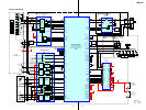
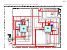
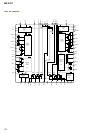
• IC BLOCK DIAGRAMS
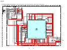
IC901 XPC18A32FCR2
Note on Schematic Diagram: MAIN SECTION
• All capacitors are in µF unless otherwise noted. pF: µµF
50 WV or less are not indicated except for electrolytics
and tantalums.
• All resistors are in Ω and
1
/
4
W or less unless otherwise
specified.
•
f
: internal component.
Note: The components identified by mark 0 or dotted
line with mark 0 are critical for safety.
Replace only with part number specified.
• : B+ Line.
• Power voltage is dc 1.5V and fed with regulated dc power
supply from battery terminal.
• Voltages and waveforms are dc with respect to ground
under no-signal conditions.
no mark : PLAY
• Voltages are taken with a VOM (Input impedance 10 MΩ).
Voltage variations may be noted due to normal produc-
tion tolerances.
• Waveforms are taken with a oscilloscope.
Voltage variations may be noted due to normal produc-
tion tolerances.
• Circled numbers refer to waveforms.
• Signal path.
F : Analog
J : Digital
• Replacement of IC601 used in this set requires a special
tool.
• The voltage and waveform of CSP (chip size package)
cannot be measured, because its lead layout is different
form that of conventional IC.
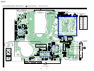
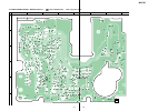
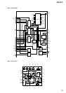
Note on Printed Wiring Boards: MAIN SECTION
• X : parts extracted from the component side.
• : Pattern from the side which enables seeing.
(The other layers' patterns are not indicated.)
Caution:
Pattern face side: Parts on the pattern face side seen from the
(Side B) pattern face are indicated.
Parts face side: Parts on the parts face side seen from the
(Side A) parts face are indicated.
• Main boards is four-layer pritnted board.
However, the patterns of layer 2 and 3 have not been
included in this diagrams.
• Replacement of IC601 used in this set requires a special
tool.
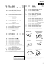
• Lead Layouts
Lead layout of
conventional IC
surface
CSP (chip size package)
56
55
42 41
40
VLON
XWK1
XWK2
XWK3
XWK4
VSTV
7
VRMC
GND
8
VL
VLO
9 10
VL
11
L2
12
PGND2
13
PGND2
VIF
VA
VAFB
VDFB
VIFFB
GND
VC
VCO
VCOUT
L1
VC
NC
PGND1
PGND1
14
15
16
17
18
19
20
39 38 37 36 35
34 33 32 31 30 29
28
27
26
25
24
23
22
21
1
2
3 4
5
6
54
53
52
51
50
49
48
47
46
45
44
43
L1
RF1
INM1
DTC1
DTC2
RF2
INM2
PWM1
PWM2
VG
LG
PGND2
L2
NC
NC
VD
VC2
XRST
CRST
RSTREF
VREF
VB
GND
CLKSEL
VAIFON
FFCLR
SLEEP
CLK
SERIAL PASS
REGULATOR VA
SERIAL PASS
REGULATOR VD
SERIAL PASS
REGULATOR VIF
BANDGAP
REFERENCE
VC
XRST (INT)
VC
VC
VSTB VC VB
POWER
SWITCH 1
VG
STEP-UP
PRE DRIVEER
VG
STEP-UP
PRE DRIVEER
PWM
VG
VC
VG
VG
VC
STEP-UP
DC/DC
CONVERTOR
START-UP
VCVB
VB
VG
VG
STEP-UP
PRE DRIVEER
PWER
SWITCH 2
VG
VC VB
VC
VSTB
CONTROL
VC
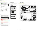
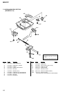
MAIN BOARD SUB ASSY
• Audio board is supplied with main board sub ASSY.
• Audio board can not be moved away from main bord.
Give a damage when take it off forcibly.
• The part that audio board overlap with main board can not
be repaired.
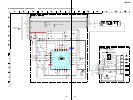
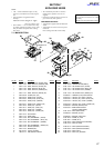
• WAVEFORMS
1
IC501 1 TE
2
3
IC501 ed (RF)
IC501 rs (FE)
Approx.
12 mVp-p
Approx.
1.2 Vp-
p
Approx.
10 mVp-p
Ver 1.1 2001.12