


1-48 (No.49793)
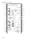
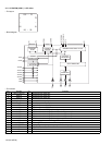
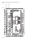
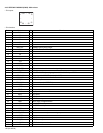
4.16 TC94A14FA (IC1621) : DSP & DAC
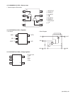
• Terminal layout & block daiagram
• Pin function
LPF
1-bit
DAC
Clock
generator
Micro-
controller
interface
Audio out
circuit
Digital
output
Address
circuit
Correction
circuit
16 k
RAM
CLV servo
Digital equalizer
automatic
adjustment circuit
Servo
control
A/D
D/A
PWM
Synchronous
guarantee
EFM
decoder
Sub code
decoder
PLL
TMAX
VCO
Data
slicer
ROM
RAM
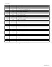
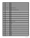
49
48 47 46 45 44 43 42 41 40 39
38 37 36 35 34 33
32
31
30
29
28
27
26
25
24
23
22
21
20
19
18
17
161514131211101 2 3 4 5 6 7 8 9
50
51
52
53
54
55
56
57
58
59
60
61
62
63
64
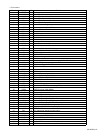
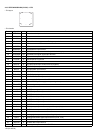
Pin
No
Symbol I/O Descroption
1 BCK O Bit clock output pin.32fs48fsor 64fs selectable by command.
2 LRCK O L/R channel clock output pin."L" for L channel and "H" for R channel.
Output polarity can be inverted by command.
3 AOUT O Audio data output pin. MSB-first or LSB-first selectable by command.
4 DOUT O Digital data output pin.Outputs up to double-speed playback.
5 IPF O Correction flag output pin. When set to "H" AOUT output cannot be corrected by C2 correction processing.
6V
DD3
- Digital 3.3V power supply voltage pin.
7V
SS3
- Digital GND pin.
8 SBOK O Subcode Q data CRCC result output pin. "H" level when result is OK.
9 CLCK O Subcode P-W data read I/O pin. I/O polarity selectable by command.
10 DATA O Subcode P-W data output pin.
11 SFSY O Playback frame sync signal output pin.
12 SBSY O Subcode block sync signal output pin. "H" level at S1 when subcode sync is detected.
13 HSO
I/O General-purpose input / output pins.Input port at reset.
14 UHSO
15 PV
DD3
- PLL-only 3.3V power supply voltage pin.
16 PDO O EFM and PLCK phase difference signal output pin.