


2000 Feb 09 20
Philips Semiconductors Product specification
2 × 25 W high efficiency car radio power
amplifier
TDA1563Q
APPLICATION NOTES
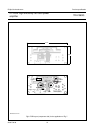
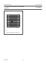
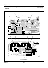
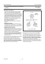
Example of the TDA1563Q in a car radio system
solution
The PCB shown here is used to demonstrate an audio
system solution with Philips Semiconductors devices for
car audio applications. The board includes the SAA7705H:
a high-end CarDSP (Digital Signal Processor), the
TDA3617J: a voltage regulator providing 9 V, 5 V and
3.3 V outputs, and two TDA1563Qs to provide four 25 W
power outputs. A complete kit (application report, software
and demo board) of this “car-audio chip-set demonstrator”
is available.
The TDA1563Q is a state of the art device, which is
different to conventional amplifiers in power dissipation
because it switches between SE mode and conventional
BTL mode, depending on the required output voltage
swing. As a result, the PCB layout is more critical than with
conventional amplifiers.
NOTES AND LAYOUT DESIGN RECOMMENDATIONS
1. The TDA1563Q mutes automatically during switch-on
and switch-off and suppresses biasing clicks coming
from the CarDSP circuit preceding the power amplifier.
Therefore, it is not necessary to use a plop reduction
circuit for the CarDSP. To mute or to enlarge the mute
time of the system, the voltage at the mode pin of the
amplifiers should be kept between 2 V and 3 V.
2. The input reference capacitor at pin 3 is specified as
1 µF but has been increased to 10 µF to improve the
switch-on plop performance of the amplifiers. By doing
this, the minimum switch-on time increases from
standby, via internal mute, to operating from 150 ms to
600 ms.
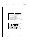
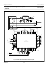
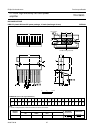
3. It is important that the copper tracks to and from the
electrolytic capacitors (SE capacitors and supply
capacitors) are close together. Because of the
switching principle, switching currents flow here.
Combining electrolytic capacitors in a 4-channel
application is not recommended.
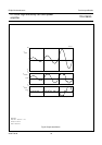
4. Filters at the outputs are necessary for stability
reasons. The filters at output pins 8 and 10 to ground
should be connected as close as possible to the
device (see layout of PCB).
5. Connect the supply decoupling capacitors of 220 nF
as closely as possible to the TDA1563Qs.
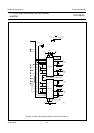
6. Place the tracks of the differential inputs as close
together as possible. If disturbances are injected at the
inputs, they will be amplified 20 times. Oscillation may
occur if this is not done properly.
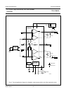
7. The SE line output signal of the CarDSP here is
offered as a quasi differential input signal to the
amplifiers by splitting the 100 Ω unbalance series
resistance into two 47 Ω balanced series resistances.
The return track from the minus inputs of the amplifiers
are not connected to ground (plane) but to the line out
reference voltage of the CarDSP, VrefDA.
8. The output signal of the CarDSP needs an additional
1st order filter. This is done by the two balanced series
resistances of 47 Ω (see note 7) and a ceramic
capacitor of 10 nF. The best position to place these
10 nF capacitors is directly on the input pins of the
amplifiers. Now, any high frequency disturbance at the
inputs of the amplifiers will be rejected.
9. Only the area underneath the CarDSP is a ground
plane. A ground plane is necessary in PCB areas
where high frequency digital noise occurs. The audio
outputs are low frequency signals. For these outputs,
it is better to use two tracks (feedand return) asclosely
as possible to each other to make the disturbances
common mode. The amplifiers have differential inputs
with a very high common mode rejection.
10. The ground pin of the voltage regulator is the
reference for the regulator outputs. This ground
reference should be connected to the ground plane of
the CarDSP by one single track. The ground plane of
the CarDSP may not be connected to “another” ground
by a second connection.
11. Prevent power currents from flowing through the
ground connection between CarDSP and voltage
regulator. The currents in the ground from the
amplifiers are directly returned to the ground pin of the
demo board. By doing this so, no ground interference
between the components will occur.