


TDA8566_6 © NXP B.V. 2007. All rights reserved.
Product data sheet Rev. 06 — 15 October 2007 8 of 21
NXP Semiconductors
TDA8566
2 × 40 W/2 Ω stereo BTL car radio power amplifier
7.6 Differential inputs
The input stage is a high-impedance fully differential balanced input stage that is also
capable of operating in a single-ended mode with one of the inputs capacitively coupled to
an audio ground. It should be noted that if a source resistance is added (input voltage
dividers) the CMRR degrades to lower values.
8. Limiting values
9. Thermal characteristics
Table 5. Limiting values
In accordance with the Absolute Maximum Rating System (IEC 60134).
Symbol Parameter Conditions Min Max Unit
V
P
supply voltage operating - 18 V
non-operating - 30 V
load dump protection;
during 50 ms; t
r
≥ 2.5 ms
-45V
I
OSM
non-repetitive peak output
current
-10A
I
ORM
repetitive peak output
current
- 7.5 A
T
stg
storage temperature −55 +150 °C
T
vj
virtual junction temperature - 150 °C
T
amb
ambient temperature −40 +85 °C
V
psc
short-circuit safe voltage - 18 V
V
rp
reverse polarity voltage - 6.0 V
P
tot
total power dissipation - 60 W
Table 6. Thermal characteristics
Thermal characteristics in accordance with IEC 60747-1.
Symbol Parameter Conditions Typ Unit
R
th(j-c)
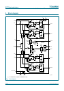
thermal resistance from junction to case see Figure 7 1.3 K/W
R
th(j-a)
thermal resistance from junction to ambient in free air 40 K/W
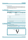
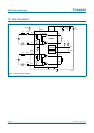
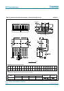
Fig 7. Equivalent thermal resistance network
001aaa155
2.2 K/W 2.2 K/W
0.2 K/W
case
output 1
virtual junction
output 2