


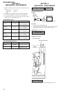
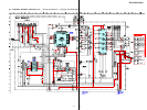
13
XR-CA400/CA410
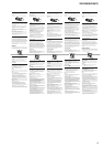
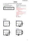
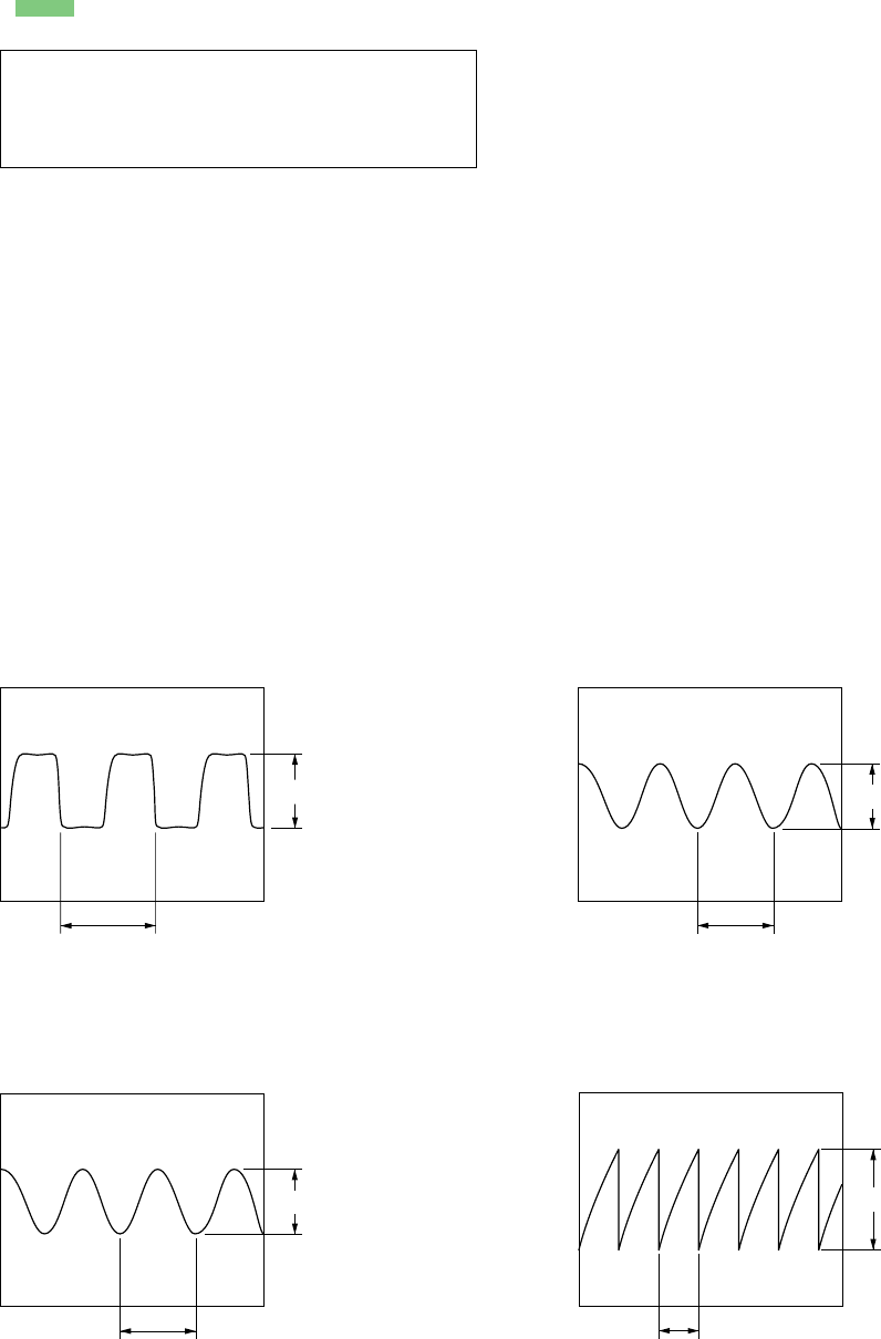
2.6 Vp-p
27.4
µ
s
3.4 Vp-p
54.4 ns
5 Vp-p
232 ns
2.3 Vp-p
30.8
µ
s
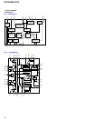
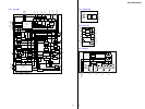
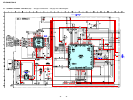
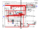
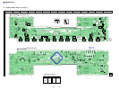
SECTION 6
DIAGRAMS
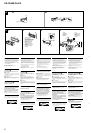
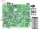
6-1. NOTE FOR PRINTED WIRING BOARDS AND SCHEMATIC DIAGRAMS
Note on Schematic Diagram:
• All capacitors are in µF unless otherwise noted. pF: µµF
50 WV or less are not indicated except for electrolytics
and tantalums.
• All resistors are in Ω and
1
/
4
W or less unless otherwise
specified.
• C : panel designation.
• A : B+ Line.
• Power voltage is dc 14.4V and fed with regulated dc power
supply from ACC and BATT cords.
• Voltages and waveforms are dc with respect to ground
under no-signal (detuned) conditions.
no mark : FM
( ) : MW/LW
〈〈 〉〉 : TAPE PLAYBACK
∗
: Impossible to measure
• Voltages are taken with a VOM (Input impedance 10 MΩ).
Voltage variations may be noted due to normal produc-
tion tolerances.
• Waveforms are taken with a oscilloscope.
Voltage variations may be noted due to normal produc-
tion tolerances.
• Circled numbers refer to waveforms.
• Signal path.
F : FM
f : MW/LW
E : TAPE PLAYBACK
L : BUS AUDIO IN
Note on Printed Wiring Board:
• X : parts extracted from the component side.
• Y : parts extracted from the conductor side.
• : Pattern from the side which enables seeing.
(The other layers' patterns are not indicated.)
Caution:
Pattern face side: Parts on the pattern face side seen from
(Conductor Side) the pattern face are indicated.
Parts face side: Parts on the parts face side seen from
(Component Side) the parts face are indicated.
• Waveforms
– MAIN Board –
1 IC51 4 (OSCO)
2 IC501 qs (OSCOUT)
3 IC501 qh (XOUT)
– KEY Board –
4 IC901 y; (OSC)