


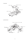

HCD-SD1
– 21 – – 22 –
THIS NOTE IS COMMON FOR PRINTED WIRING
BOARDS AND SCHEMATIC DIAGRAMS.
(In addition to this, the necessary note is printed
in each block.)
For schematic diagrams.
Note:
• All capacitors are in µF unless otherwise noted. pF: µµF
50 WV or less are not indicated except for electrolytics
and tantalums.
• All resistors are in Ω and
1
/
4
W or less unless otherwise
specified.
•
¢
: internal component.
• 2 : nonflammable resistor.
• 1 : fusible resistor.
• C : panel designation.
For printed wiring boards.
Note:
• X : parts extracted from the component side
• p : parts mounted on the conductor side.
•
®
: Through hole.
•
¢
: internal component.
• b : Pattern from the side which enables seeing.
(The other layers' patterns are not indicated.)
• S : B+ Line.
• T : B– Line.
• H : adjustment for repair.
• Voltages and waveforms are dc with respect to ground in
service mode.
• Voltages are taken with a VOM (Input impedance 10 MΩ).
Voltage variations may be noted due to normal produc-
tion tolerances.
• Waveforms are taken with a oscilloscope.
Voltage variations may be noted due to normal produc-
tion tolerances.
• Circled numbers refer to waveforms.
Signal path.
F : FM
E : PB (MD)
m : PB (TAPE)
n : REC
J : CD
c : digital out
• Abbreviation
SP : Singapore model.
HK : Hong Kong model.
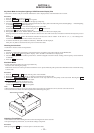
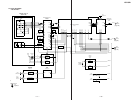
WAVEFORMS
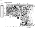
– BD SECTION –
• Indication of transistor
Caution:
Pattern face side: Parts on the pattern face side seen from the
(Side B) pattern face are indicated.
Parts face side: Parts on the parts face side seen from the
(Side A) parts face are indicated.
C
These are omitted
EB
Q
C
These are omitted
EB
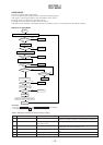
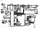
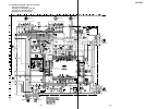
– MAIN SECTION –
1
IC701 !¡ (XI)
1
2
3
IC101 #¡ (RFO) (PLAY Mode)
500 mV/DIV, 500 ns/DIV
IC101 $¢ (TEI) (PLAY Mode)
50 mV/DIV, 1 µs/DIV
4
5
6
7
IC103 3 (MDP) (PLAY Mode)
IC103 @• (RFCK)
IC103 @™ (BCLK)
IC103 @∞ (XPCK)
Approx.
100 mVp-p
IC101 2 (FEI) (PLAY Mode)
50 mV/DIV, 1 µs/DIV
2.6 Vp-p
7.6 µs
5.1 Vp-p
136 µs
5 Vp-p
474 ns
5.1 Vp-p
22.8 µs
8
IC103 @º (LRCK)
9
IC104 6 (XTO)
4.6 Vp-p
16.9344 MHz
2
IC701 !¢ (XI)
2.6 Vp-p
32 kHz
4.3 Vp-p
5 MHz
1.3 ± 0.3 Vp-p
Approx.
150 mVp-p
5.3 Vp-p
14 ns
Note: The components identified by mark ! or dotted line
with mark ! are critical for safety.
Replace only with part number specified.