


SPRZ153
TMS320C6201 Silicon Errata
6
2 Changes to the TMS320C6201 Data Sheet (literature number SPRS051)
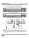
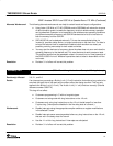
Table 2. Timing Requirements for Interrupt Response Cycles
NO
C6201B
UNIT
NO.
MIN MAX
UNIT
4 t
d(CKO2L-IACKV)
Delay time, CLKOUT2 low to IACK valid –4 6 ns
5 t
d(CKO2L-INUMV)
Delay time, CLKOUT2 low to INUMx valid 6 ns
6 t
d(CKO2L-INUMIV)
Delay time, CLKOUT2 low to INUMx invalid –4 ns
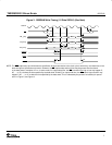
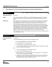
Table 3. JTAG Test-Port Timing
NO.
C6201,
C6201B
UNIT
NO.
MIN MAX
UNIT
1 T
c(TCK)
Cycle time, TCK 50 ns
4 T
h(TCKH-TDIV)
Hold time, TDI/TMS/TRST valid after TCK high 9 ns
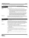
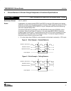
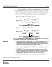
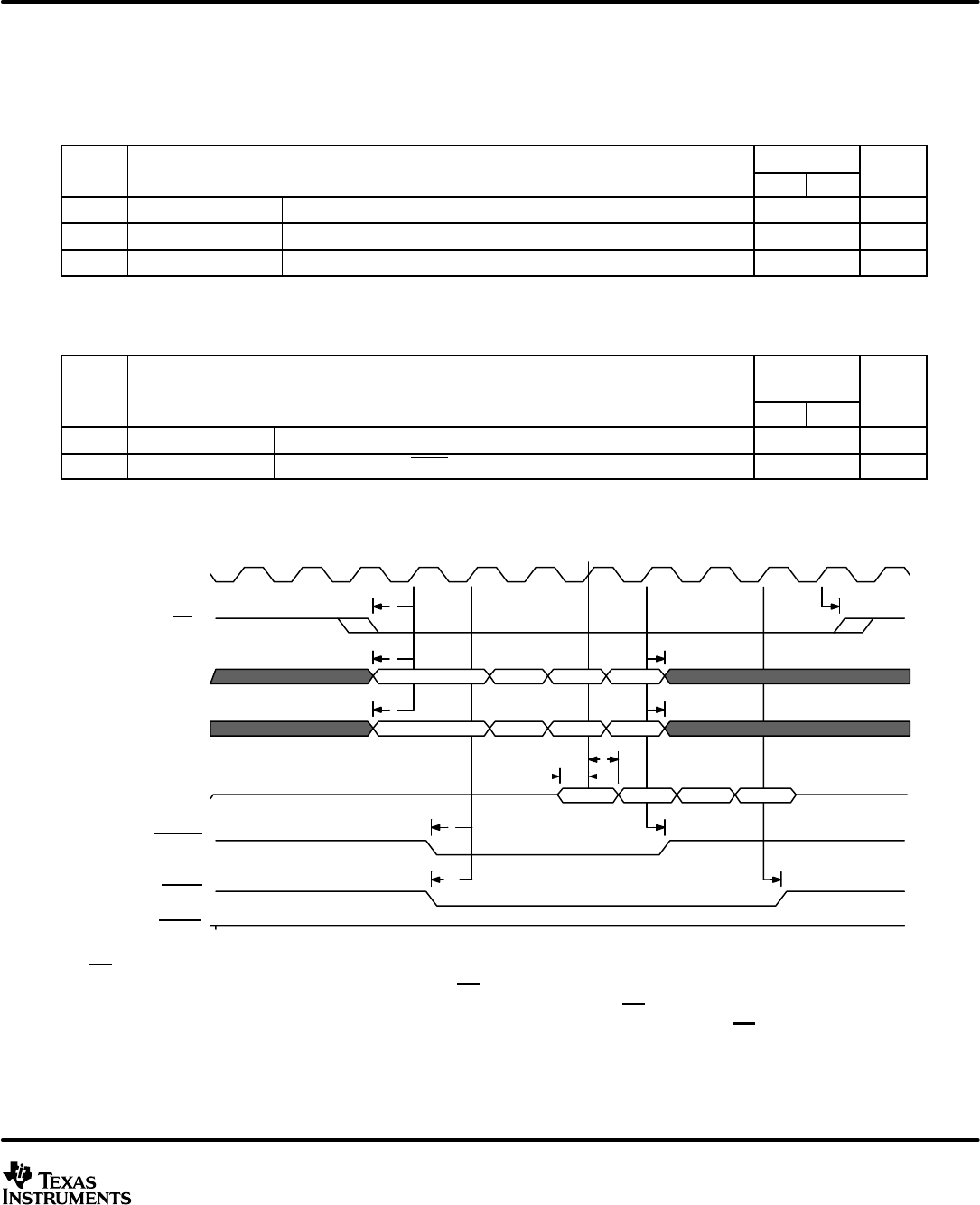
Figure 2. SBSRAM Read Timing (1/2 Rate SSCLK) (See Note)
BE1 BE2 BE3 BE4
A1 A2 A3 A4
Q1 Q2 Q3 Q4
1211
109
65
43
21
8
7
SSCLK
BE_ [3:0]
EA [21:2]
ED [31:0]
CE
SSADS
SSOE
SSWE
NOTE: The CEx output setup and hold times are specified to be accurate relative to the clock cycle to which they are referenced, since
these timings are specified as minimums. However, the CE
output setup and hold time may be greater than that shown
in the data sheet in multiples of P ns. In other words, for output setup time, the CE
x transition from high to low may happen P,
2P, …, or nP ns before the time specified by the data sheet. Similarly, for output hold time, the CE
x low-to-high transition may
happen P, 2P, …, or nP ns after the time specified by the data sheet. This is indicated by the period of uncertainty for specs 1
and 2 in Figure 2, and Figure 3.