


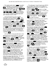
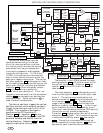
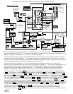
The diode modulator controls the horizontal yoke
current which affects the horizontal size. This is
accomplished by the diode forward current. In effect,
the diode shorts out the horizontal width coil to the
extent of the diode forward current during the previous
horizontal trace time. The current used to control the
diode forward current comes from the diode modulator
and is controlled by the control circuit and the
switching mode driver.
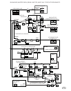
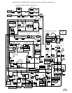
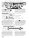
HORIZONTAL RASTER WIDTH CONTROL CIRCUIT DESCRIPTION.
The beam current from the FBT is converted to a
voltage by resistors 009 and is filtered by capacitor
010 . Resistor 097 then connects the signal to the
current node of the control amplifier, which
accomplishes the blooming correction function.
The horizontal size voltage from the remote control
PCB 490 is applied directly to the current node
(LM392 Pin 5) of the control amplifier by resistor 043 .
The horizontal width control circuit is comprised of
two main parts; The control circuit and the diode
modulator (DM). The control circuit combines four
signals in the monitor to produce the width control
circuit. These signals are:
3. Correct horizontal raster distortion caused by
periods of high beam current.
2. Correct pincushion distortion in the vertical axis.
1. Provide a convenient means for adjusting
the horizontal raster size.
The purpose of the horizontal width control is to:
4. EHT return on the FBT
Vertical yoke return.3.
V. current feedback resistor2.
H. Size Pot.1.
Beam current - - - - - - -
Vertical parabolic + Iv
Vertical current (Iv) - -
Horizontal size - - - - - -
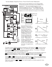
For pincushion correction, two separate signals are
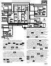
used. The inverted vertical current waveform
(TP 34) and the yoke return waveform (TP 33). The
yoke return waveform includes a parabolic and linear
component. The inverse of the linear component is
added to the yoke return waveform to correct the
pincushion. The vertical current waveform (Iv) is
inverted by an Op Amp and resistors 029 and 051 .
Resistor 031 level shifts the inverted Iv to + 6V.
The (vertical parabolic + Iv) is AC coupled by capacitor
082 and resistor 038 and 040 . It is then
amplified by an Op Amp connected as a voltage
follower. Resistor 038 protects the Op Amp against
arc related voltage spikes. Load resistors 050 and
053 prevent cross over distortion of the Op Amps by
using only the current source transistors.
The inverted Iv and (parabolic voltage +Iv) are added
to the current node of the control amplifier by resistors
041 , 042 , 030 , & 052 which then makes up the
pincushion correction signal.
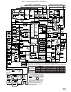
The power output stage of the horizontal width
control circuit is a high efficiency switching mode
driver. The FBT pulse is integrated by capacitor
057
through resistor 095 and level shifted by resistor 058
to produce a saw tooth waveform. See waveform block
TP 39. By connecting one input of the comparator, in
the LM392 049 , to this sawtooth signal and the other
input to the control amplifier a switched signal with a
duty cycle dependent on the control voltage is
produced at the output. Resistors 055 and 056 form
a voltage divider which limits the control voltage
amplitude to be within the sawtooth waveform.
Resistor 060 acts as a pullup for the comparator
output. Resistor 461 couples the power MOSFET 460
to the comparator. Capacitor 463 and resistor 464
are connected as a snubber circuit to reduces noise due
to rapid drain transitions.
When the MOSFET is on (gate voltage high)
current increases in inductor 458 and when the
MOSFET is turned off the current is dumped in to the
24-27V line through diode 462 . The magnitude of
this current, from the diode modulator, is determined
by the duty cycle of the MOSFET which is a function
of the control voltage.
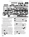
Diodes 477 and 478 with current equalizing
resistors
475 and 476 rectify the flyback waveform
present on the GND referenced node of the
horizontal tuned circuit. This current is conducted
through inductor
457 and integrated by capacitor
456 and then is controlled by the driver circuit.
Diodes 477 and 478 are the diode modulator
diodes and the forward current which the drive
circuit controls is the current which determines the
turn on delay of the GND referenced node of the
horizontal tuned circuit. An increase in the current
of diodes 477 and 478 produces a greater delay in
the GND referenced node, and reduces the amplitude
of the flyback pulse at this node, which results in an
increased horizontal size.
Capacitors 441 and 442 are the primary
horizontal tuning capacitors and must be the specified
value for a given chassis horizontal frequency and
yoke combination for proper operation of the monitor.
Capacitors
437 and
439 are the diode modulator horizontal tuning
capacitors. Diodes 440 and 438 clamp the GND
referenced node voltage to GND. Horizontal linearity
coil 431 stores energy from the flyback pulse and
injects it into the horizontal yoke in the reverse
direction of the yoke current to decrease deflection at
the start of trace to balance the decreased deflection at
the end of the horizontal trace due to I R losses in the
yoke during trace time. Capacitor 432 and resistor
428 keeps the linearity coil from ringing after retrace.
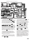
The raster may be shifted by making solder
connections: left SL or right SR . The amount of the
shift is set by solder connections S1 , S2 , & S4 .
Inductor
447 permits only the DC current to pass to
the yoke return. Resistors
423 , 424 , & 425 define
the size of the shift together with the V+ plus 5V and
V+ minus 5V supplies. Resistor 189 supplies a load
on the V+ ±5V lines to avoid over-voltage of the filter
capacitors. Resistors 185 , 195 act as fuses to protect
the PCB in the case where both SL and SR
connections are made.
These circuits are designed around a virtual ground,
the +6 volt line. This line is generated by buffering a
voltage divider
022 and 023 with an OP Amp.
Resistor
021 and capacitor 026 form the output filter.
490
2
029 051
031
040038
038
082
050
053
041
043
042 030 052
009
010
097
095
058
055
056
460
464
463
461
060
049
458
462
457
456
441 442
440
438
431
432
428
447
423 424 425
185 195
189
057
S1 S4S2
SL
SL SR
SR
84
022 023
026
021
437
439
477 478
475 476
477
478
477 478