


2.15K2.15K
1.87K
1N4148
10
R
VC
4
RED
INPUT
11.5-12.5V
VC
3
GND
U
B
o
R
o
G
o GAIN
M
+ EN
A
IN
BG
IN
R
IN R
R
R
G
A
- BL
4-7VDC
5-9Vpp
62,B4
Vs
5
VC
G
GREEN
INPUT
6
B
VC
BLUE
INPUT
1.62K
15.8K
GND
+12V
261
293
260 244 245
076
604Ω 1.21K
1.62K
ST
2.7K
064
258
1.21K
288
271
278
286
1N4148
270
277
284
1N4148
268
276
4
TTL
BL
B
GND
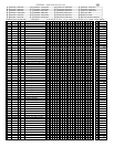
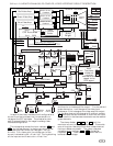
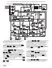
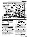
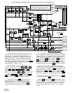
Controls XRC5346A
R
B
241
5
12
311
+12V
274
PN2222
273275
0
VC
228
0Ω
GND
+12V
GND
292
0Ω
12V
100uF
267
+
21 1415 7 8
0Ω
218
412Ω
30Ω
272
3.92K
75Ω
75Ω 75Ω
75Ω 75Ω
75Ω
84.5Ω
0Ω
243
242
264
K
B5
75.0Ω
0Ω
225
223
226
J
A5
88.7Ω
0Ω
+12V
233
234
231
232
L
205Ω
A5
265
GND
56pF
221
10K
070
0Ω
219
PN2222
16 13 9 6
084
086
FDH400
213
FDH400
FDH400
TC 3 Blue
TC5 Green
TC7 Red
To Video Board
Blanking & Beam Current Limit
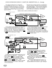
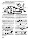
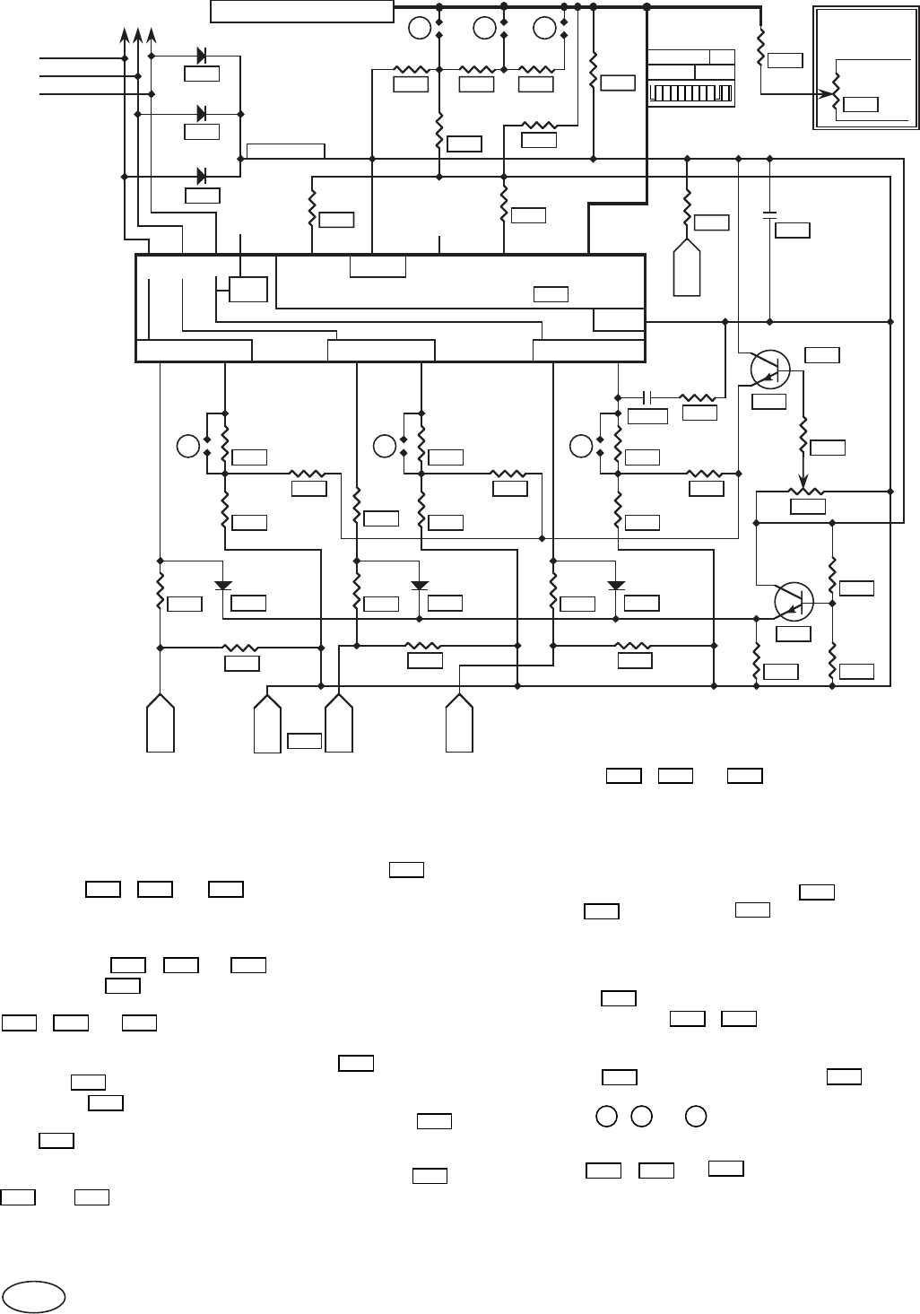
0V to .7V, POSITIVE ANALOG, DC COUPLED, VIDEO INTERFACE CIRCUIT DESCRIPTION.
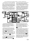
VIDEO GAIN
LINE
062
1K
485
1K
RC2
Remote
Control
+12V
M. GAIN
GND
PCB
GND
GND
GND
15.8K* 15.8K* 15.8K*
*Replace
221 with a
0Ω jumper
for fixed
black level.
For DC coupled positive analog video signals, the
signal source black level is 0 volts. The standard
saturated color voltages are .7 volt and 1 volt.
The RGB video signals and sync are connected to
the monitor through the video input connector 292 .
Resistors 288 , 286 , & 284 terminate the video
lines and load the input such that, when no signal
source is connected, the screen is dark.
Resistors 278 , 277 , & 276 protect the video
interface IC 241 from transients. They also act as
load resistors for the clamp diodes. The clamp diodes
271 , 270 , & 268 limit the peak amplitude of the
video, to prevent overdrive of the video amplifiers.
These diodes are connected to transistor
274 and load
resistor
275 . The base to emitter voltage of the
transistor 274 balances the clamp diode’s forward
voltage for temperature compensation. Resistors
272
and 273 set the clamp voltage.
The gain of the input circuit is set by resistors
226 ,
264 , & 232 .
Resistors 223 , 242 , & 231 produce a voltage drop
across the gain resistors to offset the voltage drop
caused by the .6mA bias current across the input and
protection resistors. +12 volts to these resistors
produces a fixed black level. An optional black level
adjustment may replace the +12V with a range of
0 volts to 11.3 volts. Potentiometer 070 is buffered by
transistor
221 and resistor 219 which provide the
adjustment voltage.
The master gain line is connected to the video
interface IC
241 at pin 12. It multiplies the gain set
by the gain resistors
225 , 226 , etc. by 0 to 1.
Vertical and horizontal blanking set the gain to 0
during retrace. The gain is adjusted by the master
gain control
485 through load resistor 062 . The
maximum gain may also be limited by making solder
connections S , T , & U .
Diodes
084 , 086 , & 067 clamp the video lines
connected to the video board to prevent damage to the
video interface IC from arc related voltage spikes.
66
241
268
278 277 276
292
284286288
232264
273
274
275
270271
223
062
219
225
241
226
272
274
070
221
231242
084
086
213
226
S
T
U
485