


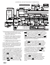
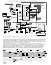
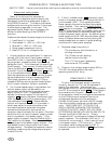
The FET 136 works together with the
transformer 166 to provide a low resistance
current path from V- to GND. This low
resistance coupled with no large voltage times
current products is what makes the power
supply efficient. Resistor 137 provides a
means for sensing the FET current. In the low
current mode, it is used to set the 300mA current
and in the full on mode it is used to
The FET drive is always off during the
negative slope of the oscillator, or just after the
sync pulse. Since the FET drive pulse is started
by the error amplifier voltage and terminated by
the end of the oscillator cycle, a control system
via pulse width modulation has been established.
The oscillator waveform is produced by charging
capacitor 102 with a constant current set by
resistor J7 to a voltage of 5V and then
discharging the capacitor with double the
charging current to 2.5V. Adding the flyback
pulse, via capacitor 123 to this waveform
synchronizes the oscillator, since the oscillator
frequency is set below the horizontal frequency.
Resistors J2 , J4 and capacitor 108 limit the
error amplifier's AC gain, to hold the control loop
stable. Capacitor 107 holds the error amplifier
stable. Capacitor 110 reduces power supply
noise, but, if too large, will cause the power
supply to be unstable. The 127V line is adjusted
by making solder connections on the J PRA (refer
to page 65 for the layout)
. Solder connections JC
and JD are used to raise the 127V line up to 4.5
volts in steps of 1.5 volts. Connections JA and JB
lower the 127V line as much as 4.5V.
The series regulator IC
115 , controls
current to the monitor GND by pulse width
modulation. A PNP transistor
112 , has an
emitter current, that is directly proportional to
the 127V line voltage due to resistor
J1 and
adjustment resistors J13 & J14 . This
current is transmitted to the power supply V-
line, and is applied to a resistor J5 , J15 , &
J16 . The voltage across these resistors is
compared to a reference voltage by the error
amplifier. If the +127V line goes up the output
of the error amplifier voltage goes up.
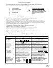
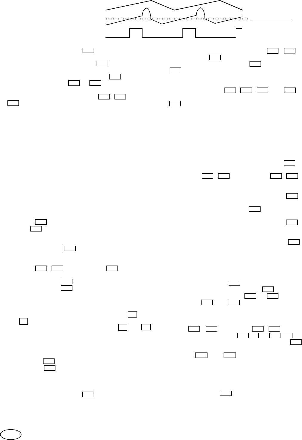
The pulse width modulation, which controls the
+ 127V line voltage, is accomplished by turning
the FET drive on at some particular voltage
along the rising slope of the oscillator waveform.
This particular voltage is the error amplifier
output voltage. See waveforms above.
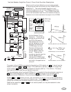
SWITCH MODE POWER SUPPLY CIRCUIT DESCRIPTION.
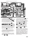
Oscillator waveform with sync:
FET drive, C5184 pin 10:
Error Amp. V.
Fet Drive
With Sync
Oscillator waveform without sync:
sense the max. current. Resistors 140 , 133
and capacitor 138 reduce power supply
electrical noise. Transistor
127 and diode
116 short the FET drive to V- when the
monitor is turned off to protect the FET from
conducting current with a still large drain
voltage. Resistors J10 , J11 , J12 and 134
provide a means for checking flyback diode
142 conduction via a comparator. If the
comparator measures low flyback diode voltage
the FET is turned on to the .3A low current
mode. This mode is necessary for power up,
since initially the +127V line is 0V and no
reverse diode voltage exists. The over voltage
protect circuit, at pin 14, has a trip voltage of
8V and when it is activated, it shuts down the
power supply. The EHT is measured by
rectifying the flyback pulse, with diode 130 ,
from a secondary winding of the FBT.
Capacitors 125 , 124 and resistors 126 , J9
are connected as a low pass filter to smooth out
the simulated EHT voltage which is then
applied to the C5184 at pin 14. Resistor J8
protects the IC current sense input from
voltage spikes and resistor 113 protects the
PNP transistor from momentary overvoltage
damage due to line spikes. Zener diode 181
protects the horizontal and video circuits from
overvoltage due to power supply failure. If the
+127V line exceeds 160V, the zener diode 181
shorts to GND the +127V line.
At the input to the power supply is a
voltage doubler which outputs between 240 to
425VDC depending on the AC line voltage. It
has a three amp fuse 146 to protect the PCB
traces, an inrush current limiter 159 to
protect the rectifier diodes 148 & 156 .
Capacitors 150 and 155 are used to reduce
diode noise from the monitor to the AC input.
For 220VAC operation the voltage doubler is
replaced by a full wave rectifier by adding
diodes 151 , 154 , capacitors 152 , 153 and
removing the jumper at 152 . 144 & 163
are the raw DC filter capacitors. Resistor J6
supplies the power supply start current and
resistors 143A and 143B balances the series
connected filter capacitors for 220VAC
operation.
Caution! When working on a monitor with a
degaussing relay, 468 unplug the degaussing coil
to avoid causing the residual current relay to
close on a cold posistor. This can happen if the
24V line is energized by a external power supply.
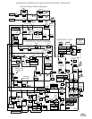
90
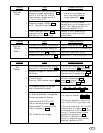
126 J9125 124
J7
J10
142
J12 134
127
140
138
133
J11
102
J16
J14
J15J5
137
166
136
J13
115
110
130
107
J2
J4
108
181
J8
113
112
J1
123
116
181
JC
JD
JA JB
146
159
148 156
155
150
151 154
144
153152
152
143B143A
163
J6
468