


1
14
Bias Control Line
from Auto Bias IC
+12V
C5346
VIDEO
INTERFACE
2SA1370
2SC3467
301
Ω
K2
1.50K
K34
3904
681Ω
K6
1.49K
40.2K
K19
K9
5.62K
885
MPS2907
18
K14
+
NE592
7
606
K7
Ω
K11
945
16V
+9.25V line
K4
15Ω
B14
140Ω
K16
560Ω
K17
12.1K
K15
120V
127V
.015uF
K1
K6
836Ω
K10
OUTPUT
2N
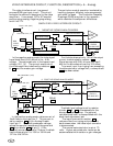
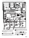
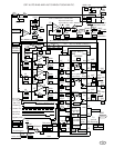
VIDEO AMPLIFIER CIRCUIT, FUNCTION, DESCRIPTION.
The video amplifier, is a high speed push pull
amplifier, which can swing as much as 90 volts.
The maximum dynamic output swing is limited to
60 volts. The rest of the output voltage range is
reserved for bias adjustment.
SIMPLIFIED VIDEO
AMPLIFIER CIRCUIT:
The voltage swing at the output is 60 volts
for a 10 mA current signal from the C5346.
For this same 10 mA current signal, the
voltage swing at the video amplifier input is
1.5 volts and the input voltage swing at the
NE592 is .80 volts. The reason for using the
voltage divider K6 and K7 is that the C5346
minimum output voltage is 7.7 volts, and the
bias voltage at the NE592 input is 5.3 volts.
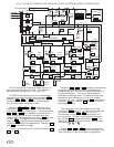
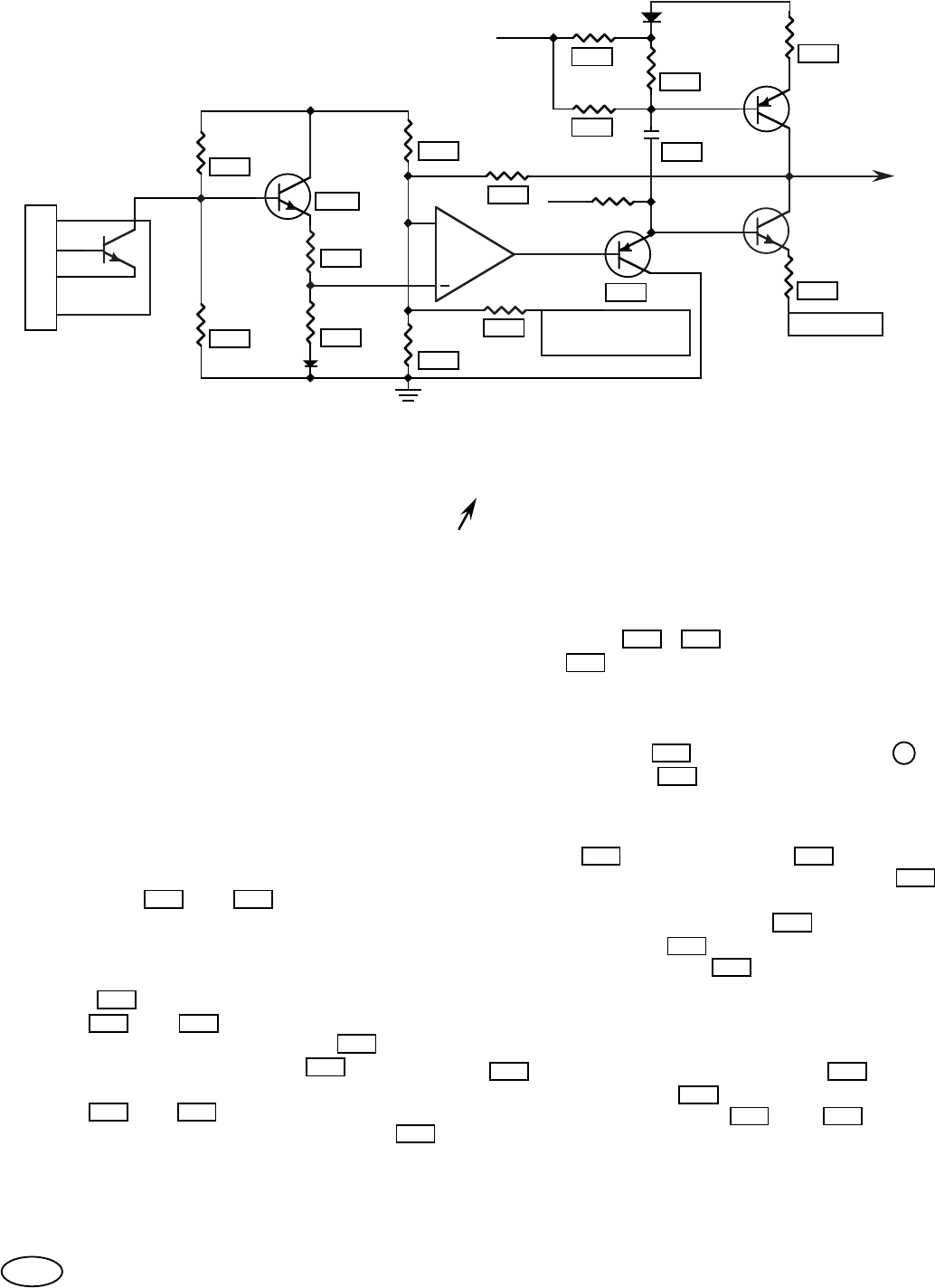
VIDEO AMPLIFIER CIRCUIT DESCRIPTION
The video amplifier's output voltage, with
no input signal, is the black level which is the
picture tube cut off voltage. This voltage is set,
for each of the three video amplifiers, by the
auto bias circuit via the bias control line. This
black level voltage has a range of 80V to 110V.
The video amplifier drive circuit is built on a
ceramic substrate which is a good heat sink.
The printed resistors and conductors are small
and have precise geometries which output a
faithful reproduction of the input signal with
good high frequency response and low overshoot.
The NE592 is a 120MHz emitter coupled
differential amplifier which is connected to a
push pull output stage. This output stage
has a low bias current of 3mA and a
bandwidth of 25MHz. Although at 25MHz,
the output stage current increases to 15mA.
The input signal is buffered by a NPN
transistor K34 for low input capacitance.
Resistors K1 and K2 set the black level
input voltage at 10 volts. Resistor
K21 (see
schematic next page) and diode
K36 protect
the input against arc related transients.
Resistors
K6 and K7 are used to set the
input bias voltage for the NE592. Diode
K35
acts as a temperature compensator to match
the emitter to base diode in the
buffer transistor.
The negative feedback circuit consists of
bias resistors
K9 , K10 and output feedback
resistor K19 . The geometry of the feedback
circuit defines the AC negative feedback path.
The autobias output, which adjusts the black
level voltage, is also connected to this node
through resistor
K11 . Solder connection A
connects resistor K22 , which raises the video
amp. output voltage by 10V, for some CRTs.
The voltage gain of the differential
amplifier K32 is set by resistor K8 . The
output of the amplifier has a load resistor
K5
for faster low going transitions and is
buffered by a PNP transistor 945 with base
matching resistor
K20 . The load resistor for
this buffer amplifier is
K3 which is
connected to the 16 volt line.
The buffered output of the differential
amplifier is DC coupled to the NPN transistor
943 and AC coupled, by capacitor 885 , to
the PNP transistor 951 of the push-pull
output stage. Resistors K18 and 953
protect the push-pull transistors from current
spikes caused by voltage transients when CRT
arcing occurs.
68
K6
K21
K36
K1 K2
K34
K7
K9
951
943
K35
K7K6
945
K5
K8K32
K22
K11
K10
K19
K18
953
885
K3
K20
A