


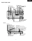
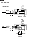
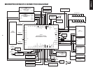
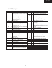

11
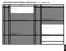
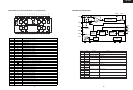
Terminal description
Pin
No.
Symbol
I/O
Description
Pin
No.
Symbol
I/O
Description
Focus error amplifier output.
Connected internally to the window comparator input
for bias adjustment.
1 FEO O
2 FEI Focus error input. I
3
4
FDFCT
I
Capacitor connection pin for defect time constant.
FGD I
Ground this pin through a capacitor for cutting the
focus servo high-frequency gain.
5
FLB
I
External time constant setting pin for boosting the
focus servo low-frequency.
6
FE_O
O
Focus drive output.
7
FE_M
I Focus amplifier inverted input.
8 SRCH
I
External time constant setting pin for generating
focus search waveform.
9
TGU
I External time constant setting pin for switching track-
ing high-frequency gain.
10
TG2
I
External time constant setting pin for switching track-
ing high-frequency gain.
11
FSET
I
Peak frequency setting pin for focus and tracking
phase compensation amplifier.
12 TA_M I Tracking amplifier inverted input.
13
TA_O
O Tracking drive output.
14
SL_P
I Sled amplifier non-inverted input.
16 SL_O O Sled drive output.
15
SL_M
I Sled amplifier inverted input.
F I-V and E I-V amplifier inverted input.
Connect these pins to photo diodes F and E.
17 ISET I Connect an external capacitance to set the current
which determines the Focus search, Track jump, and
Sled kick heights.
18
VCC
I Positive power supply.
19 LOCK I
The sled overrun prevention circuit operates when
this pin is Low. (no pull-up resistance)
20 CLK
I
22 DATA
I
21
XLT
I
Serial data transfer clock input from CPU.
(no pull-up resistance)
Latch input from CPU. (no pull-up resistance)
Serial data input from CPU. (no pull-up resistance)
23
XRST I Reset input; resets at Low. (no pull-up resistance)
24 C. OUT
O
Track number count signal output.
25
SENS1
O
Outputs FZC, DFCT1, TZC, BALH, TGH, FOH,
ATSC, and others according to the command from
CPU.
26 SENS2 O
Outputs DFCT2, MIRR, BALL, TGL, FOL, and
others according to the command from the CPU.
27
FOK
O
Focus OK comparator output.
28
CC2 I
Input for the defect bottom hold output with capa-
citance coupled.
29
CC1
O
Defect bottom hold output. Connected internally to
the interruption comparator input.
30 CB
I
Connection pin for defect bottom hold capacitor.
31 CP
I
32
RF_I
I
33 RF_O
O
34
RF_M
I
Connection pin for MIRR hold capacitor.
MIRR comparator non-inverted input.
Input for the RF summing amplifier output with capa-
citance coupled.
RF sunning amplifier output. Eyepattern check point.
RF summing amplifier inverted input.
The RF amplifier gain is determined by the resistance
connected
between this pin and RFO pin.
35 RFTC
I
External time constant setting pin during RF level
control.
36
LD O APC amplifier output.
37
PD I APC amplifier input.
38
PD1
I
39
PD2
I
RF I-V amplifier inverted input. Connect these pins
to the photo diode A + C and B + D pins.
40
FE_BIAS
I
Bias adjustment of focus error amplifier.
Leave this pin open for automatic adjustment.
41
F
I
42
I
E
43 EI
—
I-V amplifier E gain adjustment.
(When not using automatic balance adjustment)
44
VEE
—
Negative power supply.
45 TEO O
Tracking error amplifier output. E-F signal is output.
46 LPFI I Comparator input for balance adjustment.
(Input from TEO through LPF)
47
TEI
I
Tracking error input.
48
ATSC
I
Window comparator input for ATSC detection.
49
TZC
I
Tracking zero-cross comparator input.
50
TDFCT
I
Capacitor connection pin for defect time constant.
51
VC
O (VCC + VEE)/2 direct voltage output.
52 FZC
I
Focus zero-cross comparator input.
CR-305X