


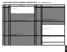

13
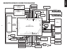
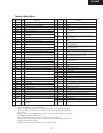
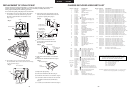
Terminal description
Pin
No.
Symbol
I/O
Description
Pin
No.
Symbol
I/O
Description
1
2
3
4
5
6
7
8
9
10
11
12
13
14
15
16
17
18
19
20
21
22
23
24
25
26
27
28
29
30
31
32
33
34
35
36
37
38
39
40
41
42
VSS
LMUT
RMUT
SQCK
SQSO
SENS
DATA
XLAT
CLOK
SEIN
CNIN
DATO
XLTO
CLKO
SPOA
SPOB
XLON
FOK
VDD
VSS
MDP
PWMI
TEST
TES1
VPCO
VCKI
V16M
VCTL
PCO
FILO
FILI
AVSS
CLTV
AVDD
RF
BIAS
ASYI
ASYO
LRCK
LRCKI
PCMD
PCMDI
—
O
O
I
O
O
I
I
I
I
I
O
O
O
I
I
O
I
—
—
O
I
I
I
O
I
O
I
O
O
I
—
I
—
I
I
I
O
O
I
O
I
GND
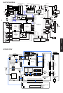
Left-channel zero detection flag.
Right-channel zero detection flag.
SQSO readout clock input.
Sub Q 80-bit serial output.
SENS output to CPU.
Serial data input from CPU.
Latch input from CPU. Serial data is latched at the
falling edge.
Serial data transfer clock input from CPU.
SENS input from SSP.
Track jump count signal input.
Serial data output to SSP.
Serial data latch output to SSP. Latched at the falling
edge.
Serial data transfer clock output to SSP.
Microcomputer extended interface (input A).
Microcomputer extended interface (input B).
Microcomputer extended interface (output).
Focus OK input.
Used for SENS output and the servo auto sequencer.
Power supply (+5V).
GND
Spindle motor servo control.
Spindle motor external control input.
TEST pin; normally GND.
TEST pin; normally GND.
Charge pump output for the wide-band EFM PLL.
VCO2 oscillation input for the wide-band EFM PLL.
VCO2 oscillation output for the wide-band EFM
PLL.
VCO2 control voltage input for the wide-band EFM
PLL.
Master PLL charge pump output.
Master PLL (slave = digital PLL) filter output.
Master PLL filter input.
Analog GND.
Master VCO control voltage input.
Analog power supply (+5V).
EFM signal input.
Constant current input of the asymmetry circuit.
Asymmetry comparator voltage input.
EFM full-swing output (low = VSS, high = VDD).
D/A interface. LR clock output f = Fs.
LR clock input.
D/A interface. Serial data output (two's complement,
MSB first).
D/A interface. Serial data input (two's complement,
MSB first).
D/A interface. Bit clock output.
D/A interface. Bit clock input.
GND
Power supply (+5V).
XUGF output. Switched to MNT1 or RFCK output
by a command.
XPLCK output. Switched to MNT0 output by a com-
mand.
GFS output. Switched to MNT3 or XRAOF output
by a command.
C2PO output. Switched to GTOP output by a com-
mand.
Crystal selector input. Low: 16.9344MHz;
high: 33.8688MHz.
4.2336MHz output. 1/4 frequency-divided VCKI out-
put in CAV-W mode.
Digital Out output.
Outputs a high signal when the playback disc has
emphasis, and a low signal when there is no emphasis.
Inputs a high signal when de-emphasis is on, and a
low signal when de-emphasis is off.
WFCK output.
Outputs a high signal when either subcode sync S0
or S1 is detected.
Sub P to W serial output.
SBSO readout clock input.
GND
Power supply (+5V).
Mute input. Active when high.
Analog GND.
Analog power supply (+5V).
Left-channel analog output.
Left-channel operational amplifier input.
Left-channel LINE output.
Analog GND.
Power supply for master clock.
Crystal oscillation circuit input. Input the external
master clock via this pin.
Crystal oscillation circuit output.
GND for master clock.
Analog GND.
Right-channel LINE output.
Right-channel operational amplifier input.
Right-channel analog output.
Analog power supply (+5V).
Analog GND.
System reset. Reset when low.
Power supply (+5V).
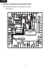
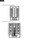
43
44
45
46
47
48
49
50
51
52
53
54
55
56
57
58
59
60
61
62
63
64
65
66
67
68
69
70
71
72
73
74
75
76
77
78
79
80
O
I
—
—
O
O
O
O
I
O
O
O
I
O
O
O
I
—
—
I
—
—
O
I
O
—
I
O
—
O
I
O
—
—
I
—
BCK
BCKI
VSS
VDD
XUGF
XPCK
GFS
C2PO
XTSL
C4M
DOUT
EMPH
EMPHI
WFCK
SCOR
SBSO
EXCK
VSS
VDD
SYSM
AVSS
AVDD
AOUT1
AIN1
LOUT1
AVSS
XVDD
XTAI
XTAO
XVSS
AVSS
LOUT2
AIN2
AOUT2
AVDD
AVSS
XRST
VDD
• PCMD is an MSB first, two's complement output.
• GTOP is used to monitor the frame sync protection status. (High: sync protection window open.)
• XUGF is the frame sync obtained from the EFM signal, and a negative pulse. It is the signal before
sync protection.
• XPLCK is the inverse of the EFM PLL clock. The PLL is designed so that the falling edge of XPLCK
and the EFM signal transition point coincide.
• GFS goes high when the frame sync and the insertion protection timing match.
• RFCK is derived with the crystal accuracy. This signal has a cycle of 136µs (during normal speed).
• C2PO represents the data error status.
• XRAOF is generated when the 16K RAM exceeds the ±4F jitter margin.
Notes)
CR-305X