


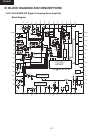
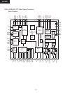
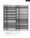
CR-305X
9
NO.
1
2
3
4
5
6
7
8
9
10
11
12
13
14
15
16
17
18
19
20
21
22
23
24
25
26
27
28
29
30
31
32
33
34
35
36
37
38
39
40
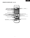
MICROPROCESSOR TERMINAL DESCRIPTION (Q701 : MPD78042GF-3B9)
Function
4G
5G
6G
7G
8G
9G
10G
VDD
CDCLK
XLT
CDDATA
SENS20
DSPMUT
SQCK
SENS
SQSO
RESET
STEREO
SD
AVSS
VOLDOWN
VOLUP
AREA
IN/OUT
SIGNAL
K1
KO
AVDD
AVREF
POFF
XT2
VSS
X1
X2
RCLK
RDATA
FREQCAL
FCE
PLLCE
I/O
O
O
O
O
O
O
O
I
O
O
O
I
O
O
I
I
I
I
I
I
O
O
-
I
I
I
I
I
I
I
I
O
I
I
I
O
O
O
O
O
Grid output pins. (4G 10G)
Power supply pin.
Command output pin to transfer the clock signal to signal processing IC(CXD2589Q).
Command output pin to transfer the latch signal to signal processing IC(CXD2589Q).
Command output pin to transfer the data signal to signal processing IC(CXD2589Q).
Sense signal input pin from servo IC(CXA1992)
Digital mute output pin to signal processing IC(CXD2589Q).
Subcode reading clock output pin to signal processing IC(CXD2589Q).
Sense signal input pin from signal processing IC(CXD2589Q).
Subcode data input pin from signal processing IC(CXD2589Q).
System reset input pin.
FM stereo broadcast detection input pin.
Broadcast detection input pin.
Ground pin for A/D converter.
Volume control output pin.
Volume control output pin.
Not used.
Initialization input pin for destination switch.
Input pin for CD tray open/close detection switches.
Signal level input pin for automatic memory.
Operation key connection pin.
Operation key connection pin.
Power supply pin for A/D converter.
Reference voltage input pin for A/D converter.
Power failure input pin.
Sub clock connection pin. Not used.
Gound pin.
Master clock connection pin.
Master clock connection pin.
Serial clock output pin to PLL and function switch ICs (TC9273,TC9162).
Serial data output pin to PLL and function switch ICs(TC9273,TC9162).
Frequency output terminal for clock adjustment
Serial latch output pin to function switch ICs(TC9273,TC9162).
Serial latch output pin to PLL IC.
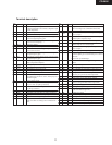
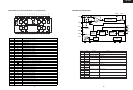
NO.
41
42
43
44
45
46
47
48
49
50
51
52
53
54
55
56
57
58
59
60
61
62
63
64
65
66
67
68
69
70
71
72
73
74
75
76
77
78
79
80
Function
POWER AMP
RDSDATA
RDSSIG
SCOR
RDSSCK
SYSIN
REMIN
IC
SYSOUT
TUMUT
ANGMUT
VDD
POWERCD
LED1
XRST
CDAUTOADJ
OPEN
CLOSE
LED2
P1
P2
P3
P4
P5
P6
P7
P8
P9
P10
P11
VLOAD
P12
P13
P14
P15
P16
P17
1G
2G
3G
I/O
O
I
I
I
I
I
I
I
O
O
O
I
O
O
O
I
O
O
O
Output pin for power supply control of power amplifier
Data input pin from RDS decoder IC.
Signal input pin from RDS decoder IC.
Sub code frame detection input pin from signal processing IC(CXD2589Q).
Clock input pin from RDS decoder IC.
System code input pin.
Signal input pin for remote controller.
Internal connection pin. Not used.
System code output pin.
Muting control signal output pin for tuner section.
Muting control signal output pin for amplifier section.
Power supply pin.
Output pin for power supply control of CD section.
Acoustic presence indicator (red) control output pin.
Reset signal output pin of signal processing IC and servo IC.
Set pin of self adjustment ON/OFF of CD
CD tray open control output pin.
CD tray close control output pin.
Acoustic presence indicator (green) control output pin.
Segment output pins. (P1 P11)
Power supply pin for FL tube.
Segment output pins. (P12 P17)
Grid output pins. (1G 3G)
Description
Description