


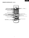
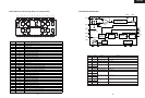

15
16
Vcc
1
2
3
4
5
6
7
8
9
10
11
12
13
14
15
30
29
28
27
26
25
24
23
22
21
20
19
18
17
16
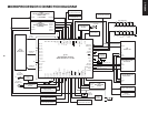
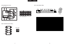
Level shift
4
BTL AMP
4
Level shift
1
BTL AMP
1
BTL AMP
3
BTL AMP
2
Level shift
3
Level shift
2
RESET
Regulator
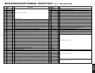
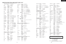
Pin No. Pin Name Description (Function)
1V
CC
Power supply (shorted with pin 30)
2 Mute ON/OFF control for all BTL AMP outputs
3V
IN
1 BTL AMP 1 input
4 VG1 BTL AMP 1 input (for gain control)
5V
O
1 BTL AMP 1 output (non-inverting side)
6V
O
2 BTL AMP 1 output (inverting side)
7 GND GND (minimum electric potential)
8 GND GND (minimum electric potential)
9 GND GND (minimum electric potential)
10 V
O
3 BTL AMP 2 output (inverting side)
11 V
O
4 BTL AMP 2 output (non-inverting side)
12 VG2 BTL AMP 2 input (for gain control)
13 V
IN
2 BTL AMP 2 input
14 REG OUT Connection for collector of external transistor (PNP); 5 V supply output
15 REG IN Connection for base of external transistor (PNP)
16 RES
Reset output
17 C
D
Reset output delay time setting (with capacitor)
18 V
IN
3 BTL AMP 3 input
19 VG3 BTL AMP 3 input (for gain control)
20 V
O
5 BTL AMP 3 output (non-inverting side)
21 V
O
6 BTL AMP 3 output (inverting side)
22 GND GND (minimum electric potential)
23 GND GND (minimum electric potential)
24 GND GND (minimum electric potential)
25 V
O
7 BTL AMP 4 output (inverting side)
26 V
O
8 BTL AMP 4 output (non-inverting side)
27 VG4 BTL AMP 4 input (for gain control)
28 V
IN
4 BTL AMP 4 input
29 V
REF
Reference voltage input for level shift circuit
30 V
CC
Power supply (shorted with pin 1)
Vcc
Vref
VIN4
VG4
Vo8
Vo7
GND
GND
GND
Vo6
Vo5
VG3
VIN3
CD
RES
Vcc
Mute
VIN1
VG1
Vo1
Vo2
GND
GND
GND
Vo3
Vo4
VG2
VI2
Reg OUT
Reg IN
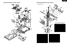
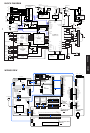
Q102:LA6541D (4-channel ridge Driver for Compact Dizcs)
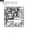
Q180:BU1923 (RDS Decoder(
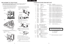
+
(4)
(3)
(5)
(6)
(12)
(11)
(16)
(1)
(2)
(10)
(9)
Measurement
circuit
Differential
decoder
Bi-phase
decoder
PLL
1187.5 Hz
PLL
57 kHz
RDS/ARI
Reference
clock
(13) (14)
(7)
(8)
120 k
100 k
100 k
Analog
Power supply
Digital
power supply
anti-aliasing
filter
8ch Switched
capacitor filter
Comparator
RCLK
QUAL
RDATA
T2T1
XO
X1
VSS2
VDD2
VSS1
VDD1
VREF
MUX
VSS3
CMP
Pin name
Demodulator quality
Demodulator data
Reference voltage
Input
Analog power supply
GND
Comparator input
Test input
Digital power supply
Crystal oscillor
-
Demodulator clock
Function
Good data : High , bad data : Low
Refer to output data trimming
1/2 VDD1
Composite signal input
4.5 V to 5.5 V
-
C-junction
Open or connected to ground
4.5 V to 5.5 V
Connects to 4.332 MHz oscillator
-
1187.5 Hz clock
Pin No.
1
2
3
4
5
6
7
8
9
10
11
12
13
14
15
16
Symbol
QUAL
RDATA
Vref
MUX
VDD1
Vss1
Vss3
CMP
T2
T1
VDD2
Vss2
XI
XO
(NC)
RCLK
CR-305X