


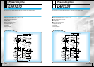
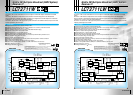
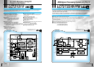
LC72711WLC72711W
MPXIN
XIN
Vssa
Vdda
XOUT
RST
CLK16
DATA
BCK
FCK
FLOCK
BLOCK
STNBY
Vssd
Vddd
IOCNT1
DACK
DREQ
IOCNT2
CRC4
FLOUT
CIN
VREF
CS
RD
WR
RDY
INT
BUSWD
TIN
SP
A3
DO
A2/DI
A1/CE
A0/CL
D0 to D15
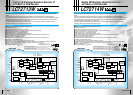
LC72711LWLC72711LW
LPFLPF
MPXIN
7.2MHz7.2MHz
Vref
Vref
XIN
Vssa
Vdda
XOUT
RST
CLK16
DATA
BCK
FCK
FLOCK
BLOCK
STNBY
Vssd
Vddd
LPF
76kHz
BPF
(SCF)
76kHz
BPF
(SCF)
VrefVref
IOCNT1
DACK
DREQ
IOCNT2
CRC4
FLOUT
CIN
VREF
CS
RD
WR
RDY
INT
BUSWD
TIN
SP
A3
DO
A2/DI
A1/CE
A0/CL
D0 to D15
63 Car Audio 64 Car Audio
Overview
Functions
Overview
Functions
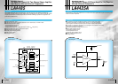
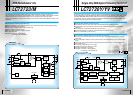
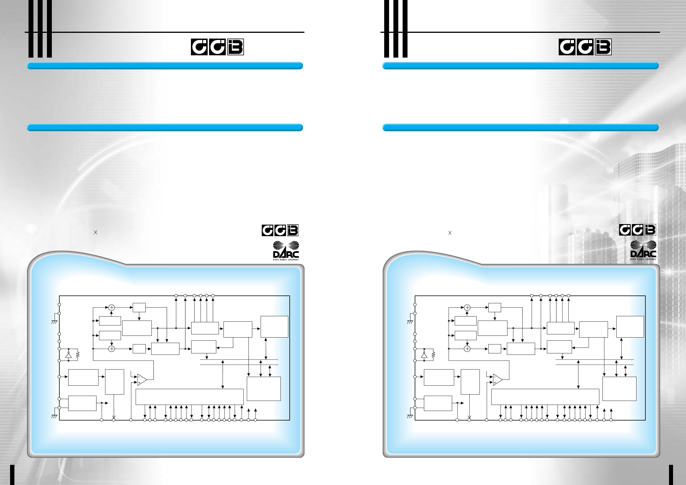
Block Diagram Block Diagram
The LC72711W is a data demodulation IC for the reception of mobile FM multiplex broadcasts in the DARC
system.
The LC72711W includes a bandpass filter for the extraction of the DARC signal from the FM baseband.
This IC is optimal for worldwide FM multiplex products since it supports all of the FM multiplex frame structures
(methods A, A', B, and C) in the ITU-R recommendations.
The LC72711W and LC72711LW support both parallel connection and CCB serial interface in place of the CPU
interface provided by the LC72709E.
The DARC (Data Radio Channel) FM multiplex broadcast technology was developed by NHK
(Japan Broadcasting Corporation).
DARC is a registered trademark of NHK Engineering Services, Inc. (NHK-ES).
A separate contract with NHK-ES is required for the manufacturer or sale of electronic
equipment that uses DARC technology.
The logo shown here may be used with electronic equipment that uses DARC technology.
■ Adjustment-free SCF based 76 kHz bandpass filter
■ Supports all FM multiplex frame structures (methods A, A', B, and C) under CPU control
■ MSK delay detection circuit using a 1T delay
■ Error correction function using a 2T delay (in the MSK detection stage)
■ Digital PLL based clock regeneration circuit
■ Shift register type 1T and 2T delay circuits
■ Block and frame synchronization detection circuits
■ Function for setting the allowable BIC error count and synchronization protection count
■ Error correction using (272,190) codes
■ Layer 4 CRC code checking circuit
■ Includes the frame memory and memory control circuit required for vertical correction
■ 7.2 MHz crystal oscillator circuit
■ Two power saving modes (standby and EC stop modes)
■ Either a CPU parallel interface (DMA) or a CCB serial interface can be used
■ Supply voltage: 4.5 to 5.5 V
■ Package: SQFP64 (10 10 mm)
:CCB is SANYO's original bus format.
All bus addresses are managed by
SANYO for this format.
❋
The DARC (Data Radio Channel) FM multiplex broadcast technology was developed by NHK
(Japan Broadcasting Corporation).
DARC is a registered trademark of NHK Engineering Services, Inc. (NHK-ES).
A separate contract with NHK-ES is required for the manufacturer or sale of electronic
equipment that uses DARC technology.
The logo shown here may be used with electronic equipment that uses DARC technology.
:CCB is SANYO's original bus format.
All bus addresses are managed by
SANYO for this format.
❋
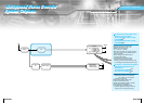
Mobile FM Multiplex Broadcast (DARC System)
Receiver IC
Mobile FM Multiplex Broadcast (DARC System)
Receiver IC
Mobile FM Multiplex Broadcast (DARC System)
Receiver IC
Mobile FM Multiplex Broadcast (DARC System)
Receiver IC
The LC72711LW is a data demodulation IC for the reception of mobile FM multiplex broadcasts in the DARC
system.
The LC72711LW includes a bandpass filter for the extraction of the DARC signal from the FM baseband.
This IC is optimal for worldwide FM multiplex products since it supports all of the FM multiplex frame structures
(methods A, A', B, and C) in the ITU-R recommendations.
The LC72711W and LC72711LW support both parallel connection and CCB serial interface in place of the CPU
interface provided by the LC72709E.
■ Adjustment-free SCF based 76 kHz bandpass filter
■ Supports all FM multiplex frame structures (methods A, A', B, and C) under CPU control
■ MSK delay detection circuit using a 1T delay
■ Error correction function using a 2T delay (in the MSK detection stage)
■ Digital PLL based clock regeneration circuit
■ Shift register type 1T and 2T delay circuits
■ Block and frame synchronization detection circuits
■ Function for setting the allowable BIC error count and synchronization protection count
■ Error correction using (272,190) codes
■ Layer 4 CRC code checking circuit
■ Includes the frame memory and memory control circuit required for vertical correction
■ 7.2 MHz crystal oscillator circuit
■ Two power saving modes (standby and EC stop modes)
■ Either a CPU parallel interface (DMA) or a CCB serial interface can be used
■ Supply voltage: 2.7 to 3.6 V
■ Package: SQFP64 (10 10 mm)
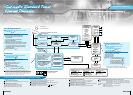
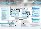
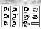
1T delay
2T delay
1T delay
2T delay
Clock
regeneration
Clock
regeneration
MSK
correction
MSK
correction
Synchronization
regeneration
PN
decoding
Synchronization
regeneration
PN
decoding
Timing
control
Timing
control
Error
correction
Layer 2 CRC
Error
correction
Layer 2 CRC
Data
Antialiasing
filter
Antialiasing
filter
Address
Memory array
Data
Address
Memory array
Output control (CPU interface) and
layer 4 CRC checking circuit
Output control (CPU interface) and
layer 4 CRC checking circuit
LPF