


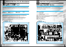
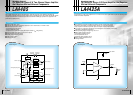
LC72723/MLC72723/M LC72720Y/YV
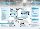
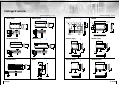
REFERENCE
VOLTAGE
ANTIALIASING
FILTER
SMOOTHING
FILTER
57kHz
BPF
(SCF)
TEST
PLL
(57kHz)
V
REF
CLOCK
RECOVERY
(1187.5Hz)
DATA
DECODER
RAM
(128 bit)
OSC
CLK(4.332MHz)
+5V +5V
Vdda
Vssa
MPXIN
TEST
X
IN
X
OUT
RDDA
RDCL
MODE
RST
RDS-ID/
READY
RDS-ID
DETECT
Vssd
Vddd
CINFLOUT
V
REF
+
-
71 Car Audio 72 Car Audio
Overview
Functions
Block Diagram
Overview
Functions
Features
The LC72723 and LC72723M are Radio Data System (RDS) demodulation and signal-processing ICs.
These ICs integrate a bandpass filter, the demodulation circuit, and data buffer RAM on the same chip and allow
the RDS data to be read out in slave mode operation with an externally provided clock input signal.
(Master mode operation, in which the data is output in synchronization with the internal RDS clock output, is also
supported.)
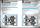
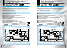
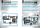
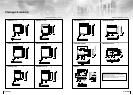
The LC72720Y and LC72720YV are single-chip system ICs that implement the signal processing required by the
European Broadcasting Union RDS (Radio Data System) standard and by the US NRSC (National Radio System
Committee) RDBS (Radio Broadcast Data System) standard. These ICs include band-pass filter, demodulator,
synchronization, and error correction circuits as well as data buffer RAM on chip and perform effective error
correction using a soft-decision error correction technique.
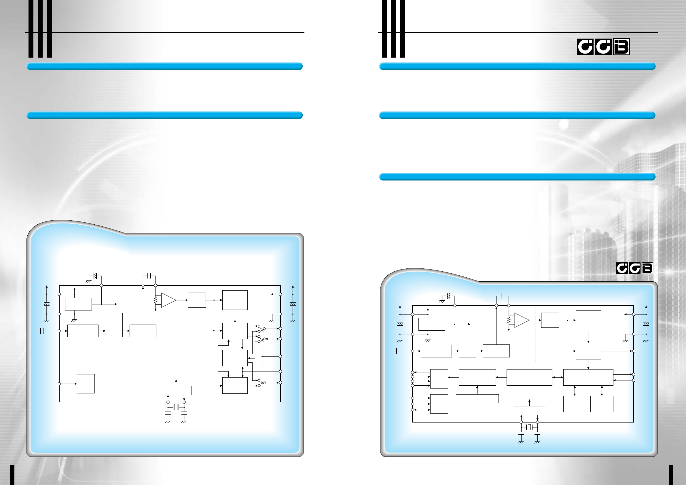
RDS Demodulator ICsRDS Demodulator ICs
■ Bandpass filter: switched capacitor filter (SCF)
■ RDS demodulation: 57 kHz carrier regeneration, clock regeneration, biphase and differential decoding
■ Buffer RAM: 128 bits (about 100 ms)
■ Data I/O: Data readout in either master or slave mode
■ RDS ID detection: Supports ID reset
■ Standby mode: The crystal oscillator is stopped
■ Fully adjustment free
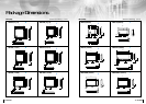
■ Packages:(LC72723) : DIP16(300mil)
(LC72723M) : MFP16(225mil)
■ Error correction capability improved by soft-decision error correction
■ The load on the control microprocessor can be reduced by storing decoded data in the on-chip data
buffer RAM
■ Two synchronization detection circuits provide continuous and stable detection of the synchronization
timing
■ Data can be read out starting with the backward-protection block data after a synchronization reset
■ Fully adjustment free
■ Low voltage (supply voltage: 3.0 V min) type
■ Operating power-supply voltage: 3.0 to 3.6 V
■ Operating temperature: -40 to +85°C
■ Packages: (LC72720Y) : DIP24S(300mil)
(LC72720YV) : SSOP30(275mil)
■ Band-pass filter: Switched capacitor filter (SCF)
■ Demodulatior: RDS data clock regeneration and demodulated data reliability information
■ Synchronization: Block synchronization detection (with variable backward and forward protection
conditions)
■ Error correction: Soft-decision/hard-decision error correction
■ Buffer RAM: Adequate for 24 blocks of data (about 500 ms) and flag memory
■ Data I/O: CCB interface (power on reset)
REFERENCE
VOLTAGE
ANTIALIASING
FILTER
SMOOTHING
FILTER
57kHz
BPF
(SCF)
TEST
PLL
(57kHz)
V
REF
CLOCK
RECOVERY
(1187.5Hz)
DATA
DECODER
SYNC
DETECT-2
SYNC
DETECT-1
OSC/DIVIDER
MEMORY CONTROL
CLK(4.332MHz)
+3.3 V +3.3 V
Vdda
Vssa
MPXIN
T2
T3 to T7
T1
CCB
DI
CE
CL
RAM
(24 BLOCK DATA)
ERROR CORRECTION
(SOFT DECISION)
SYNC/EC CONTROLLER
DO
X
IN
X
OUT
SYR
SYNC
RDS-ID
Vssd
Vddd
CINFLOUT
V
REF
+
-
Block Diagram
Single-Chip RDS Signal-Processing System ICSingle-Chip RDS Signal-Processing System IC
:CCB is SANYO's original bus format.
All bus addresses are managed by
SANYO for this format.
❋