


SiI 141B SiI-DS-0037-C
Silicon Image, Inc. 2 Subject to Change without Notice
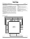
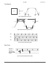
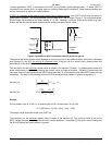
Functional Block Diagram
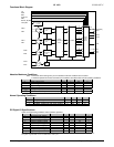
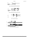
Absolute Maximum Conditions
Note: Permanent device damage may occur if absolute maximum conditions are exceeded.
Functional operation should be restricted to the conditions described under Normal Operating Conditions.
Symbol Parameter Min Typ Max Units
V
CC
Supply Voltage 3.3V -0.3 4.0 V
V
I
Input Voltage -0.3 V
CC
+ 0.3 V
V
O
Output Voltage -0.3 V
CC
+ 0.3 V
T
A
Ambient Temperature (with power applied) -25 105
°C
T
STG
Storage Temperature -65 150
°C
θ
JA
Thermal Resistance (Junction to Ambient) 45
°C /W
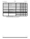
Normal Operating Conditions
Symbol Parameter Min Typ Max Units
V
CC
Supply Voltage 3.0 3.3 3.6 V
V
CCN
Supply Voltage Noise 100 mV
P-P
T
A
Ambient Temperature (with power applied) 0 25 70
°C
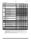
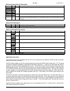
DC Digital I/O Specifications
Under normal operating conditions unless otherwise specified.
Symbol Parameter Conditions Min Typ Max Units
V
IH
High-level Input Voltage 2 V
V
IL
Low-level Input Voltage 0.8 V
V
OH
High-level Output Voltage 2.4 V
V
OL
Low-level Output Voltage 0.4 V
V
CINL
Input Clamp Voltage
1
I
CL
= -18mA GND -0.8 V
V
CIPL
Input Clamp Voltage
1
I
CL
= 18mA IVCC + 0.8 V
V
CONL
Output Clamp Voltage
1
I
CL
= -18mA GND -0.8 V
V
COPL
Output Clamp Voltage
1
I
CL
= 18mA OVCC + 0.8 V
I
IL
Input Leakage Current -10 10
µA
Note:
1
Guaranteed by design. Voltage undershoot or overshoot cannot exceed absolute maximum conditions
for a pulse of greater than 3 ns or one third of the clock cycle.
INTER-
CHANNEL
SYNC.
DECODER
CLT3
CLT2
DE2
CLT1
PLL_SYNC
DE1
VSYNC
HSYNC
DE0
8
8
8
VCR
EXT_RES
PANEL
INTER-
FACE
LOGIC
Q[35:0/23:0
]
ODCK
DE
HSYNC
VSYNC
CLT1
CLT2
CLT3
RX2+
RX2-
RX1+
RX1-
RX0+
RX0-
RXC+
RXC-
PIXS
OCK_INV
PLL
24/36
VCR
VCR
VCR
DFO
ST
SCDT
PDO
DATA
RECOVERY
CH2
DATA
RECOVERY
CH0
DATA
RECOVERY
CH1
HSYNC_DEJTR
Termination
Control