


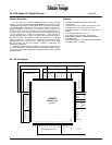
SiI 141B SiI-DS-0037-C
Silicon Image, Inc. 8 Subject to Change without Notice
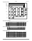
Differential Signal Data Pin Description
Pin Name Pin # Type Description
RX0+ 70 Analog TMDS Low Voltage Differential Signal input data pairs.
RX0- 71
RX1+ 67
RX1- 68
RX2+ 64
RX2- 65
RXC+ 74 Analog TMDS Low Voltage Differential Signal input clock pair.
RXC- 73
EXT_RES 76 Analog Impedance Matching Control. Resistor value should be ten times the characteristic impedance of the cable.
In the common case of 50Ω transmission line, an external 530Ω resistor must be connected between AVCC
and this pin.
Reserved Pin Description
Pin Name Pin # Type Description
RSVD 1 Out This signal must be left unconnected.
Power and Ground Pin Description
Pin Name Pin # Type Description
VCC 39 Power Core VCC, must be set to 3.3V.
50
61
GND 11 Ground Digital GND.
37
62
OVCC 15 Power Output VCC, must be set to 3.3V.
28
48
OGND 4 Ground Output GND.
13
26
46
AVCC 63 Power Analog VCC, must be set to 3.3V.
69
AGND 66 Ground Analog GND.
72
PVCC 77 Power PLL VCC, must be set to 3.3V.
PGND 78 Ground PLL GND.
Application Information
The SiI141B is pin for pin compatible with the SiI141 but includes two new features, HSYNC de-jitter and power
down when the clock is inactive.
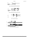
HSYNC de-jitter enables the 141B to operate properly even when the HSYNC signal contains jitter. Pin 75 is used
to enable or disable this capability (a reserved pin tied high on the SiI141). Tying this pin low enables the HSYNC
de-jitter circuitry while tying it high disables the circuitry. The HSYNC de-jitter circuitry operates normally with most
VESA standard timings. Some DOS mode resolutions do not have timings that are a multiple of eight (HSYNC
and VSYNC total times and front and back porch times are multiples of eight pixel times). If they are not a multiple
of eight, operation is not guaranteed and the HSYNC de-jitter circuitry should be turned off. When HSYNC de-
jitter is enabled, the circuitry will introduce anywhere from 0 to 7 CLK delays in the HSYNC signal relative to the
output data.
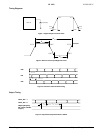
The SiI141B includes a new power saving feature, power down with clock detect circuit. The SiI141B will go into a
low power mode when there is no video clock coming from the transmitter. In this mode the entire chip is powered
down except the clock detect circuitry. During this mode digital I/O are set to a high impedance (tri-state) mode. A
weak internal pull-down device brings each output to ground. The device power down and wake-up times are
shown in Figures 6 and 7.
The SiI141B also includes a sync detect feature for pin compatibility with SiI141. In both the SiI141 and SiI141B,
SCDT goes low when DE is inactive.