


SiI 141B SiI-DS-0037-C
Silicon Image, Inc. 7 Subject to Change without Notice
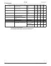
Output Pin Description
Pin Name Pin # Type Description
Q35 – Q0 See Out
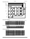
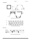
SiI 141B
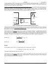
Pin
Diagram
Output Data [35:0].
Output data is synchronized with output data clock (ODCK).
When PIXS is low Q35-Q24 are low and Q23-Q0 output 24-bit/pixel data.
When PIXS is high Q17-Q0 output the even numbered pixels (pixel 0, 2, 4, ... , etc.) and Q35-Q18 output
the odd numbered pixels (pixel 1, 3, 5, ... , etc.).
Refer to the TFT Signal Mapping (SiI/AN-0008) and DSTN Signal Mapping (SiI/AN-0007) application notes
which tabulate the relationship between the input data to the transmitter and output data from the receiver.
A low level on PD or PDO will put the output drivers into a high impedance (tri-state) mode. A weak
internal pull-down device brings each output to ground.
ODCK 36 Out
Output Data Clock.
A low level on PD or PDO will put the output drivers into a high impedance (tri-state) mode. A weak
internal pull-down device brings each output to ground.
DE 41 Out Output Data Enable.
A low level on PD or PDO will put the output drivers into a high impedance (tri-state) mode. A weak
internal pull-down device brings each output to ground.
HSYNC 12 Out Horizontal Sync output control signal.
VSYNC 14 Out Vertical Sync output control signal.
CTL1 8 Out
General output control signal 1. This pin is not controlled by PDO.
CTL2 9 Out General output control signal 2
CTL3 10 Out
General output control signal 3.
A low level on PD or PDO will put the output drivers into a high impedance (tri-state) mode. A weak
internal pull-down device brings each output to ground.
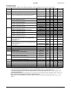
Configuration Pin Description
Pin Name Pin # Type Description
OCK_INV 80 In ODCK Polarity. A low level selects normal ODCK output, which enables data latching on the falling
edge. A high level (3.3V) selects inverted ODCK output, which enables data latching on the rising edge.
Both conditions are for color TFT panel support. For color 24-bit DSTN panel support, please refer to the
DSTN Signal Mapping (SiI/AN-0008-A) application note.
PIXS 5 In Pixel Select. A low level indicates that output data is one pixel (up to 24-bit) per clock and a high level
(3.3V) indicates that output data is two pixels (up to 36-bit) per clock.
DF0 6 In Output Data Format. This pin controls clock and data output format. A low level indicates that ODCK
runs continuously for color TFT panel support and a high level (3.3V) indicates that ODCK is stopped
(LOW) for color 24-bit DSTN panel support when DE is low. Refer to the TFT Signal Mapping (SiI/AN-
0007-A) and DSTN Signal Mapping (SiI/AN-0008-A) application notes for a table on TFT or DSTN panel
support.
HSYNC_DEJTR 75 In A low level enables the HSYNC de-jitter circuitry. A high level disables the de-jitter circuitry. If left
unconnected, the circuitry defaults to disabled.
ST 79 In Output Driver Strength. A low level indicates low drive. A high level indicates high drive.
Power Management Pin Description
Pin Name Pin # Type Description
SCDT 7 Out SyncDetect. A high level is output when DE is toggling. A low level is output when DE is inactive. See page
9.
PD 2 In Power Down (active low). A high level (3.3V) indicates normal operation and a low level indicates power down
mode. During power down mode all internal circuitry is powered down and digital I/O are set the same as
when PDO is asserted. (see PDO pin description).
PDO 3 In Power Down Output (active low). A high level indicates normal operation. A low level puts the output drivers
only into a high impedance (tri-state) mode. A weak internal pull-down device brings each output to ground.
There is an internal pull-up resistor on PDO that defaults the chip to normal operation if left unconnected.
SCDT and CTL1 are not tri-stated by this pin. See explanation of clock detect on page 8-9.