


– 33 –
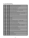
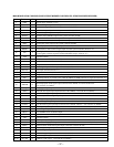
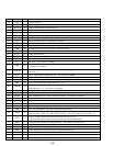
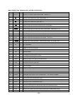
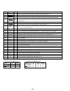
Pin No. Pin Name I/O Function
3-8. IC PIN FUNCTION DESCRIPTION
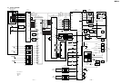
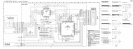
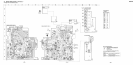
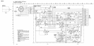
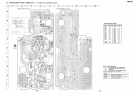
SERVO BOARD IC100 CXA1981AR (RF AMP)
1 VC O Output terminal for the center point voltage (1/2 VCC) generated
2-7 A-F I Signal input from detector circuit in the optical pick-up block
8 FI I Signal input of the operational amplifier for F signal
9 FO O Signal output of the operational amplifier for F signal
10 PD I Front monitor Connected to the photo diode
11 APCREF I Input terminal for the setting of laser power
12 TEMPI I Terminal for the connection to temperature sensor Not used this set (OPEN)
13 GND – Ground terminal
14 AAPC O LD amplifier output terminal of APC circuit
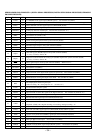
15 DAPC O Not used (OPEN)
16 TEMPR O Output terminal of the reference voltage for temperature sensor Not used this set (OPEN)
17 XRST I Reset signal input from the system controller (IC600) When reset : “L”
18 SWDT I Write data signal input from the system controller (IC600)
19 SCLK I Clock signal input from the system controller (IC600)
20 XLAT I Latch signal input from the system controller (IC600)
21 VREF O Reference voltage output Not used this set (OPEN)
22 TENV O Not used (OPEN)
23 THLD I Not used (OPEN)
24 VCC – Power supply terminal (+3.3V)
25 TFIL I Not used (OPEN)
26 TE O Tracking error signal output to CXD2535CR (IC200)
27 TLB I Input terminal of the adder signal to tracking error Not used this set (OPEN)
28 CSLED I Terminal for the sled error lowpass filter
29 SE O Sled error signal output to CXD2535CR (IC200)
30 ADFM O FM signal output terminal of the ADIP
31 ADIN I Input terminal by AC coupling is FM signal of the ADIP
32 ADAGC I External capacitor connect terminal for AGC of the ADIP
33 ADFG O ADIP double turned FM signal output to CXD2535CR (IC200) (22.05kHz ± 1kHz)
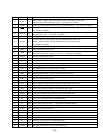
34 AUX O Sub signal output to CXD2535CR (IC200)
35 FE O Focus error signal output to CXD2535CR (IC200)
36 FLB I Input terminal of the adder signal to focus error Not used this set (OPEN)
37 ABCD O Light amount signal output to CXD2535CR (IC200)
38 BOTM O Light amount bottom hold signal output to CXD2535CR (IC200)
39 PEAK O Light amount peak hold signal output to CXD2535CR (IC200)
40 PFAGC I External capacitor connect terminal of AGC circuit for the RF
41 RF O Playback EFM RF signal output to CXD2535CR (IC200)
42 ISET I Setting terminal for the internal circuit constant 22kHz, BPF center frequency
43 AGCI I Input terminal by AC coupling is RF signal
44 RFO O RF signal output terminal
45 MORFI I Input terminal by AC coupling is RF signal of the MO
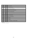
46 MORFO O RF signal output terminal of the MO
47, 48 I, J I Signal input from detector circuit in the optical pick-up block