


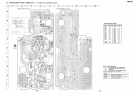
– 35 –
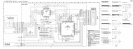
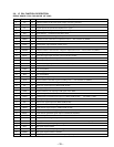
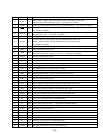
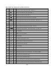
Pin No. Pin Name I/O Function
41 WFCK O
WFCK clock (7.35kHz) signal output (When playback : EFM decoder PLL system,
When recoding : EFM encoder PLL system) Not used this set (OPEN)
42 GTOP O Opens the playback EFM frame sync protection window when “H” Not used this set (OPEN)
43 GFS O
The playback EFM frame sync and interpolation protection timing match when “H”
Not used this set (OPEN)
44 XPLCK O
EFM decoder PLL clock (98Fs=4.3218MHz) signal output Falling edge of the EFM PLL clock and
the EFM signal match Not used this set (OPEN)
45 EFMO O FM signal output (When recoding) Not used this set (OPEN)
Overflow detection signal output of the internal RAM (Decoder monitor out)
46 RAOF O RAOF is signal generated when the 32k RAM exceeds the ±4F jitter margin
Not used this set (OPEN)
47 MVCI I Oscillation input for PLL of the digital in Not used this set (Fixed at “L”)
48 TEST2 I Test terminal input (Fixed at “L”)
49 DIPD O (3)
Phase comparator output for PLL of the digital in When the internal VCO : Frequency ; Low→“H”
When the external VCO : Frequency ; Low→“L” Not used this set (OPEN)
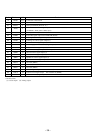
50 DVSS1 – Ground terminal (Digital system)
51 DICV I (A) Control voltage input terminal of the internal VCO for digital in PLL
52 DIFI I (A) Filter input terminal of the internal VCO for digital in PLL Not used this set (Fixed at “L”)
53 DIFO O (A) Filter output terminal of the internal VCO for digital in PLL Not used this set (OPEN)
54 AVDD1 – Power supply terminal (+3.3V) (Analog system)
55 ASYO O Playback EFM full-swing output (L=VSS, H=VDD)
56 ASYI I (A) Playback EFM asymmetry comparate voltage input terminal
57 BIAS I (A) Playback EFM asymmetry circuit constant current input terminal
58 RFI I (A) Playback EFM RF signal input from CXA1981AR (IC100)
59 AVSS1 – Ground terminal (Analog system)
60 CLTV I (A) VCO control voltage input terminal of the PLL for decoder PLL master clock
61 PCO O (3) Phase comparator output terminal of the PLL for decoder PLL master clock
62 FILI I (A) Filter input terminal of the PLL for decoder PLL master clock
63 FILO O (3) Filter output terminal of the PLL for decoder PLL master clock
64 PEAK I (A) Light amount peak hold signal input from CXA1981AR (IC100)
65 BOTM I (A) Light amount bottom hold signal input from CXA1981AR (IC100)
66 ABCD I (A) Light amount signal input from CXA1981AR (IC100)
67 FE I (A) Focus error signal input from CXA1981AR (IC100)
68 AUX1 I (A) Sub signal input from CXA1981AR (IC100)
69 VC I (A) Center point voltage (1/2 VCC) input from CXA1981AR (IC100)
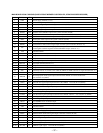
70 ADIO O (A) Monitor output of the A/D converter input signal Not used this set (OPEN)
71 TEST3 I (A) Test input terminal (Fixed at “L”)
72 AVDD2 – Power supply terminal (+3.3V) (Analog system)
73 ADRT I (A) A/D converter action limits (upper side) voltage input (Fixed at “H”)
74 ADRB I (A) A/D converter action limits (lower side) voltage input (Fixed at “L”)
75 AVSS2 – Ground terminal (Analog system)
76 SE I (A) Sled error signal input from CXA1981AR (IC100)
77 TE I (A) Tracking error signal input from CXA1981AR (IC100)
78 AUX2 I (A) Sub signal input terminal from CXA1981AR (IC100)