


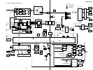

– 36 –
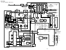
• MAIN BOARD IC100 CXD8607N (A/D CONVERTER)
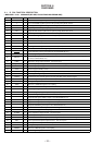
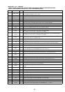
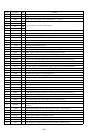
Pin No. Pin Name I/O Function
1 INRP I
R-ch analog signal (–) input terminal
2 INRM I
R-ch analog signal (+) input terminal
3 REFI I
Reference voltage (+3.3V) input terminal (for A/D converter section)
4 AVDD —
Power supply terminal (+5V) (for A/D converter section, analog system)
5 AVSS —
Ground terminal (for A/D converter section, analog system)
6 APD I
Power down detection input of the A/D converter section (for analog section) “L”: power down
7NU—
Not used (open)
8NU—
Not used (open)
9 TEST1 I
Input terminal for the test (fixed at “L”)
10 LRCK1 I
L/R sampling clock signal (44.1 kHz) input from the CXD2654R (IC121) (for A/D converter
section)
11 BCK1 I
Bit clock signal (2.8224 MHz) input from the CXD2654R (IC121) (for A/D converter section)
12 ADDT O
Recording data output to the CXD2654R (IC121)
13 V35A —
Power supply terminal (+3.3V) (for analog system)
14 VSS1 —
Ground terminal (for A/D converter section, digital system)
15
MCKI I
Master clock (256Fs=11.2896 MHz) input of the A/D converter section
16 DPD I
Reset signal input from the system controller (IC800) Reset signal is used as a detection signal
of power down to A/D converter section (digital section) “L”: reset (power down)
17 VSS2 —
Ground terminal (for D/A converter section, digital system)
18 RES I
Reset signal input terminal Reset signal is used as a initialize signal to D/A converter section
“L”: reset (initialize) Not used D/A converter section in this set
19 MODE I
Writing data input terminal Not used (fixed at “L”)
20 SHIFT I
Serial clock signal input terminal Not used (fixed at “L”)
21 XLATCH I
Serial data latch pulse signal input terminal Not used (fixed at “L”)
22 256CK O
256Fs (11.2896 MHz) clock signal output terminal Not used (open)
23 V35D —
Power supply terminal (+3.3V) (for digital system) Not used (open)
24 VSS2 —
Ground terminal (for D/A converter section, digital system)
25 512FS O
512Fs (22.5792 MHz) clock signal output terminal Not used (pull down)
26 BCK2 I
Bit clock signal (2.8224 MHz) input terminal (for D/A converter section)
Not used (fixed at “L”)
27 DADT I
Playback data input terminal Not used (fixed at “L”)
28 LRCK2 I
L/R sampling clock signal (44.1 kHz) input terminal (for D/A converter section)
Not used (fixed at “L”)
29 VDD2 —
Power supply terminal (+5V) (for D/A converter section, digital system)
Not used (fixed at “L”)
30 R1 O
R-ch PLM signal 1 output terminal Not used (open)
31 AVDDR —
Power supply terminal (+5V) (for R-ch side D/A converter section, analog system)
Not used (fixed at “L”)
32 R2 O
R-ch PLM signal 2 output terminal Not used (open)
33 AVSSR —
Ground terminal (for R-ch side D/A converter section, analog system)
34 XVDD —
Power supply terminal (+5V) (for X’tal system) Not used (open)
35 XOUT O
System clock output terminal (22 MHz) Not used (open)
36 XIN I
System clock input terminal (22 MHz) Not used (fixed at “L”)
37 XVSS —
Ground terminal (for X’tal system)
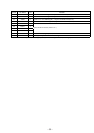
38 AVSSL —
Ground terminal (for L-ch side D/A converter section, analog system)
39 L2 O
L-ch PLM signal 2 output terminal Not used (open)