


MDS-JB920
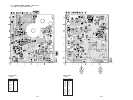
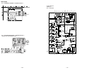
– 59 –
– 60 –
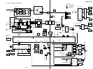
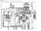
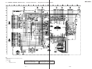
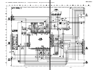
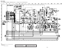
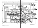
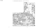
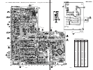
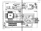
6-10. SCHEMATIC DIAGRAM – MAIN Section (3/3) – • See page 53 and 54 for Waveforms. • See page 72 and 73 for IC Block Diagrams.
Note:
• Voltages and waveforms are dc with respect to ground in
playback mode.
no mark : PB
∗
: Impossible to measure
(Page 68)
(Page 68)
(Page 58)
(Page 56)