


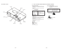

– 38 –
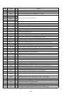
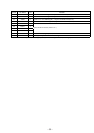
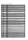
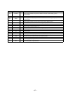
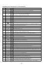
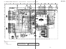
• MAIN BOARD IC800 M30610MCA-264FP (SYSTEM CONTROLLER)
Pin No. Pin Name I/O Function
1 JOG1
I
JOG dial pulse input from the rotary encoder (S713 ≠ AMS ±)
2 JOG0 I
JOG dial pulse input from the rotary encoder (S713 ≠ AMS ±)
3C1O
Monitor output terminal for the test C1 error rate is output when test mode
4
ADER
O
Monitor output terminal for the test ADER is output when test mode
5 SQSY
I
Subcode Q sync (SCOR) input from the CXD2654R (IC121)
“L” is input every 13.3 msec Almost all, “H” is input
6 RMC
I Remote control signal input from the remote control receiver (IC761)
7 AIN1
I Sircs remote control signal input of the S-LINK CONTROL A1
8 BYTE
I External data bus line byte selection signal input “L”: 16 bit, “H”: 8 bit (fixed at “L”)
9 CNVSS
— Ground terminal
10 XT-IN
I Sub system clock input terminal (32.768 kHz)
11 XT-OUT
O Sub system clock output terminal (32.768 kHz)
12 S.RST I
System reset signal input from the LA5632 (IC700) “L”: reset
For several hundreds msec. after the power supply rises, “L” is input, then it changes to “H”
13 XOUT
O Main system clock output terminal (7 MHz)
14 GND
— Ground terminal
15 XIN
I Main system clock input terminal (7 MHz)
16 +3.3V
— Power supply terminal (+3.3V)
17
NMI I Non-maskable interrupt input terminal (fixed at “H” in this set)
18 DQSY
I
Digital In U-bit CD format subcode Q sync (SCOR) input from the CXD2654R (IC121)
“L” is input every 13.3 msec Almost all, “H” is input
19 P.DOWN
I Power down detection signal input terminal “L”: power down, normally: “H”
20 XINT
I Interrupt status input from the CXD2654R (IC121)
21 DVOL1
I Digital rec level volume input terminal
22 DVOL0
I Digital rec level volume input terminal
23 to 30 NC
I Not used (fixed at “L”)
31 SWDT O
Writing data output to the CXD2654R (IC121) and D/A converter (IC200)
32 SRDT I
Reading data input from the CXD2654R (IC121)
33 SCLK O
Serial clock signal output to the CXD2654R (IC121) and D/A converter (IC200)
34 FLCS
O Chip select signal output to the FL/LED driver (IC771)
35
FLDATA O Serial data output to the FL/LED driver (IC771)
36 NC
I Not used (fixed at “L”)
37 FLCLK
O Serial data transfer clock signal output to the FL/LED driver (IC771)
38 to 47 NC
I Not used (fixed at “L”)
48 CSET0
I Destination setting terminal (US, Canadian models: fixed at “L”, AEP, UK models: fixed at “H”)
49 CSET1
I Destination setting terminal (US, Canadian models: fixed at “H”, AEP, UK models: fixed at “L”)
50 XINSW
I Setting terminal of the loading control system select (fixed at “H” in this set)
51 NC
I Not used (fixed at “L”)
52 MNT2 (XBUSY) I
Busy signal input from the CXD2654R (IC121)
53 DIG-RST O
Reset signal output to the CXD2654R (IC121) and BH6511FS (IC152) “L”: reset
54 MNT1 (SHOCK) I
Track jump detection signal input from the CXD2654R (IC121)
55 SENS
I Internal status (SENSE) input from the CXD2654R (IC121)
56 LDON O
Laser diode on/off control signal output to the automatic power control circuit “H”: laser on
57 REFLECT I
Detection input from the disc reflection rate detect switch (S102)
“L”: high reflection rate disc, “H”: low reflection rate disc
58 PROTECT I
Rec-proof claw detect input from the protect detect switch (S102) “H”: write protect