


– 37 –
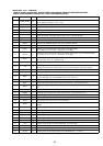
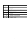
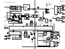
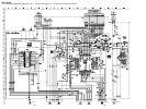
Pin No. Pin Name I/O Function
40 AVDDL —
Power supply terminal (+5V) (for L-ch side D/A converter section, analog system)
Not used (open)
41 L1 O
L-ch PLM signal 1 output terminal Not used (open)
42 VDD2 —
Power supply terminal (+5V) (for L-ch side D/A converter section, digital system)
Not used (open)
43, 44 VDD1 —
Power supply terminal (+5V) (for A/D converter section, digital system)
45 VSS1 —
Ground terminal (for A/D converter section, digital system)
46 TEST2 I
Input terminal for the test (fixed at “L”)
47 TEST3 I
Input terminal for the test (fixed at “L”)
48 VSS1 —
Ground terminal (for A/D converter section, digital system)
49 NU —
Not used (open)
50 NU —
Not used (open)
51 AVSS —
Ground terminal (for A/D converter section, analog system)
52 LVDD —
Power supply terminal (+5V) (for A/D converter section, buffer system)
53 LVSS —
Ground terminal (for A/D converter section, buffer system)
54 REFO O
Reference voltage (+3.3V) output terminal (for A/D converter section)
55 INLM I
L-ch analog signal (+) input terminal
56 INLP I
L-ch analog signal (–) input terminal