


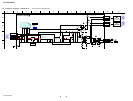
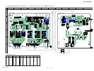
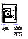

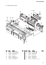
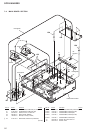
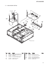

SCD-XA5400ES
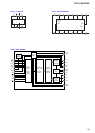
44
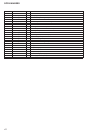
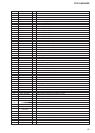
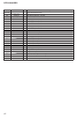
Pin No. Pin Name I/O Description
76 XROMCS O Chip select signal output to the fl ash ROM
77 HA1 O Address signal output to the fl ash ROM
78 XRD O Read enable signal output to the fl ash ROM
79, 80 HD0, HD1 I/O Two-way data bus terminal with the fl ash ROM
81 DVSS - Ground terminal
82 to 86 HD2 to HD6 I/O Two-way data bus terminal with the fl ash ROM
87 HA21 O Address signal output to the fl ash ROM
88 RESERVED - Not used
89 HD7 I/O Two-way data bus terminal with the fl ash ROM
90 DVSS - Ground terminal
91, 92 HA17, HA0 O Address signal output to the fl ash ROM
93 DVDD18 - Power supply terminal (+1.8V)
94 FWD O Loading motor drive signal output terminal Not used
95 REV O Loading motor drive signal output terminal Not used
96 DVDD3 - Power supply terminal (+3.3V)
97 IFSDO O Serial data output to the system controller
98 IFCK O Serial data transfer clock signal output to the system controller
99 xIFCS O Chip select signal output to the system controller
100 IFSDI I Serial data input from the system controller
101 SCL I Serial data transfer clock signal output to the EEPROM
102 SDA I/O Two-way data bus with the EEPROM
103 CKSW I Chucking detection switch input terminal Not used
104 OCSW I Disc table open/close detection switch input terminal Not used
105 RXD I Receive data input terminal Not used
106 TXD O Transmit data output terminal Not used
107 ICE I ICE mode enable signal input terminal Not used
108 xSYSRST I Reset signal input from the system controller "L": reset
109 RESERVED - Not used
110 xIFBSY I Busy signal input from the system controller
111 DQM0 O Data mask signal output to the SD-RAM
112 EEWP O Write protect signal output to the EEPROM
113 to 117 RD7 to RD3 I/O Two-way data bus with the SD-RAM
118 DVDD3 - Power supply terminal (+3.3V)
119 to 129
RD2 to RD0,
RD15 to RD8
I/O Two-way data bus with the SD-RAM
130 TSD_M O Thermal shut down signal output to the motor/coil driver
131 DVDD3 - Power supply terminal (+3.3V)
132 DQM1 O Data mask signal output to the SD-RAM
133 _RWE O Write enable signal output to the SD-RAM
134 _CAS O Column address strobe signal output to the SD-RAM
135 _RAS O Row address strobe signal output to the SD-RAM
136 _RCS O Chip select signal output to the SD-RAM
137, 138 BA0, BA1 O Bank address signal output to the SD-RAM
139 to 141 RA10, RA0, RA1 O Address signal output to the SD-RAM
142 DVDD18 - Power supply terminal (+1.8V)
143, 144 RA2, RA3 O Address signal output to the SD-RAM
145 DVDD3 - Power supply terminal (+3.3V)
146 DRCLK O Serial data transfer clock signal output to the SD-RAM
147 CKE O Clock enable signal output to the SD-RAM
148 DVSS - Ground terminal
149 to 155 RA11, RA9 to RA4 O Address signal output to the SD-RAM
156 DVDD3 - Power supply terminal (+3.3V)
157 MUTE123 O Muting signal output to the motor/coil driver
158 MUTE O Muting signal output to the motor/coil driver
159 DDC_DA O Serial data transfer clock signal output terminal
160 DVDD18 - Power supply terminal (+1.8V)
161 DDC_CLK I/O Two-way data bus with terminal
162 HTPLG I HDMI hot-plug detection signal input terminal
163 AGND3 - Ground terminal
164 EXT_RES - Not used