


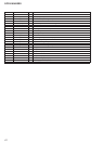
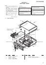
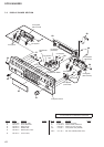
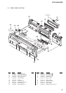
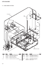
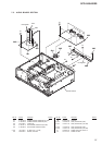
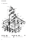
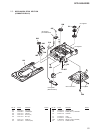

SCD-XA5400ES
46
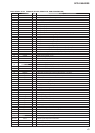
Pin No. Pin Name I/O Description
228, 229
ADACVDD1,
ADACVDD2
- Power supply terminal (+3.3V)
230 Rt/DIR_DI I Serial data input terminal Not used
231 Lt/DIR_DO O Serial data output terminal Not used
232 ADACVSS1 - Ground terminal
233 ADACVDD1 - Power supply terminal (+3.3V)
234 SADCVDD18 - Power supply terminal (+1.8V)
235 SADCVSS18 - Ground terminal
236 RFGND18 - Ground terminal
237 RFVDD18 - Power supply terminal (+1.8V)
238 XTALO O System clock output terminal Not used
239 XTALI I System clock input terminal
240 JITFO O Output terminal of the RF jitter meter
241 JITFN I Input terminal of the RF jitter meter
242 PLLVSS - Ground terminal
243 PLLVDD3 - Power supply terminal (+3.3V)
244 LPFON O Data PLL loop fi lter output terminal
245 LPFIP I Data PLL loop fi lter input terminal
246 LPFIN I Data PLL loop fi lter input terminal
247 LPFOP O Data PLL loop fi lter output terminal
248 ADCVDD3 - Power supply terminal (+3.3V)
249 ADCVSS - Ground terminal
250 RFVDD3 - Power supply terminal (+3.3V)
251 RFRPDC O RF ripple detect output terminal
252 RFRPAC I RF ripple detect input terminal
253 HRFZC I High frequency RF ripple zero crossing terminal
254 CRTPLP O Defect level fi lter capacitor connecting terminal
255 RFGND18 - Ground terminal
256 OSP O RF offset cancellation capacitor connecting terminal