


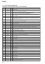
43
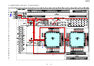
XR-M510
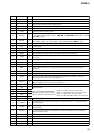
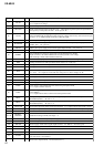
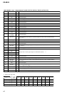
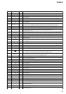
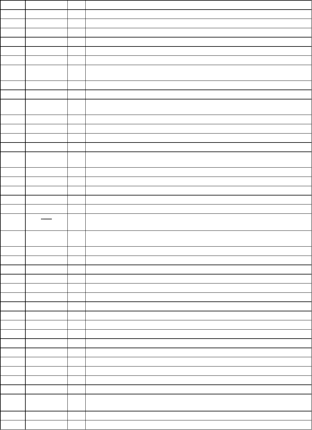
Pin No. Pin Name I/O Description
53 VSS —
Ground terminal
54, 55 NC
O Not used (open)
56 PD6
O Not used (open)
57 BOOT I
Serial data input at the flash memory writing mode “L” is input when writing change
58 VCC —
Power supply terminal (+5V)
59 NC
O Not used (open)
60
TX/LCD-DATA O
Display serial data output to the liquid crystal display driver (IC901, 902)
Output terminal for UART transfer data when writing into internal flash memory data
61 SP-SI
I Spectrum analyzer display serial data input terminal Not used (fixed at “L”)
62 RX
I Input terminal for UART transfer data when writing into internal flash memory data
63 SP-SCK
I
Spectrum analyzer display serial data transfer clock signal input terminal
Not used (fixed at “L”)
64 LCD-SCK
O Display serial data transfer clock signal output to the liquid crystal display driver (IC901, 902)
65 VSS —
Ground terminal
66 LCDCE0
O Chip enable signal output to the liquid crystal display driver (IC901) “H” active
67, 68 VSS —
Ground terminal
69 LCD-INH1
O
Blank indicate control signal output to the liquid crystal display driver (IC901, 902)
“L”: no display
70 LCDCE1
O Chip enable signal output to the liquid crystal display driver (IC902) “H” active
71 LCD-INH2
O Not used (open)
72 to 78 P27 to P21
O Not used (open)
79 P20 O
Flash memory data write control signal output terminal “H”: active
80 FWE (L) I
Flash memory data write enable signal input terminal
81 RES I
System reset signal input from the reset signal generator (IC602) and reset switch (S901, 902)
“L” is input for several 100 msec after power on, then it changes to “H”
82 NMI (H)
I
Non maskable interrupt input terminal
Connect the backup detect circuit (BU-IN pin rl) in this set
83 STBY (H)
I Hard ware standby input terminal Not used (pull down)
84 VCC —
Power supply terminal (+5V)
85 XTAL
O System clock output terminal (18.432 MHz)
86 EXTAL
I System clock input terminal (18.432 MHz)
87 VSS —
Ground terminal
88 PF7
O Not used (open)
89 VCC —
Power supply terminal (+5V)
90 to 96 PF6 to PF0
O Not used (open)
97 UNI-SO O
Serial data output to the SONY bus interface (IC501)
98 UNI-SI I
Serial data input from the SONY bus interface (IC501)
99, 100 VSS —
Ground terminal
101 UNICKI I
Serial clock signal input from the system controller (IC601)
102 P53/ADTRG
O Not used (open)
103 AVCC —
Power supply terminal (+5V) (for A/D converter)
104 VREF I
Reference voltage (+5V) input terminal (for A/D converter)
105 SPE-IN I
Peak hold voltage detect signal input from the BA3834F (IC102)
106 to 11
0
P41/AN1 to
P45/AN5
I
Not used (fixed at “L”)
111 P46/AN6/DA0 I
Not used (fixed at “L”)
112 P47/AN7/DA1 I
Not used (fixed at “L”)