


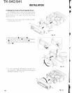
CIRCUIT
DESCRIPTION
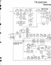
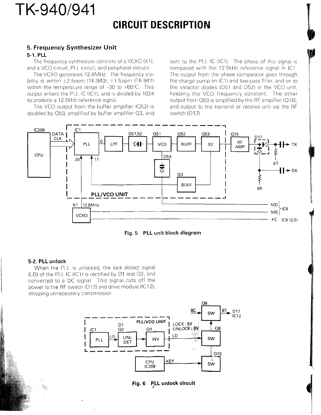
5.
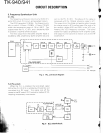
Frequency Synthesizer Unit
5-1.
PLL
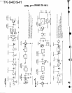
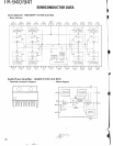
The frequency synthesizer consists of a VCXO iXl),
and
a
VCO circuit, PLL circuit, and peripheral circuits.
The VCXO generates
12.8MHz. The frequency sta-
bility
IS
withiri i2.5ppm (TK-940),
i
I
.5pprn (TK-941)
within the temperatdre range of -30 to 160°C. l~his
output enters the PLL C (ICI), and is divided by 1024
to produce a
12.5kHz reference signal.
The VCO output from the buffer amplifier
(052) is
doub!ed by 053, amplified by buffer amplifier 03, and
sen: to the PLL
IC ilC1). The phase of this signal is
compared with
?he 12.5kHz reference signal in IC1
The output from the phase coniparator goes through
the charge pump
(In ICl) and low-pass filter, and on to
the varactor diodes
(D51 and D52) in the VCO unit,
keeping the VCO frequency constant. The other
output from Q53 is amplified by the
RF
amplifier iQ181,
and output to the transmit or receive unit vla the
RF
switch (D17).
I
PLLJVCO
UNIT
-
--
---------
_I-
-
-
-
-
-
-
-
_1
I
IC209
rl
D&A
irl
__
.,__
Us
Q52 Q53
I
018 Dl7
PLL
Fig.
5
PLL unit block diagram
XI
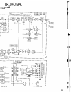
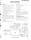
5-2.
PLL
unlock
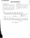
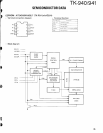
When the PLL
is
unlocked, the lock detect signal
(LD) of the PLL
IC (ICI) is rectified by Dl and Q2, and
converted
to a DC signal This signal cuts off the
power to the
RF
swltch iD17) and drive module (ICI 2),
stopping unnecessary transmission
LPF
12.8MHz
I.
Q9
LD
DET
INV SW
Fig.
6
P,LL
unlock circuit
1%
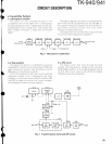
VCXO
-
IC6
MB
FC IC8 (212)
at
-
VCO
-
BUFF
-
X2
I
RF
r:
I
AMP