


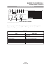

PLL
IC101 (MC1459IF) is a PLL frequency synthesizer with an on-board 1.1 GHZ divide by 64/65 dual
modulus prescaler. In addition to the prescaler and frequency counters, the synthesizer IC has a a phase
detector and a C register (Configuration register) that allows certain functions to be configured as desired.
The synthesizer is serially controlled by three wire input to the IC. Serial data is fed to pin 19 of the IC.
Serial data CLK (pin 18) and active low ENABLE (pin 17) are the input pins that allow data transfer into
the integrated circuit for control and frequency selection.
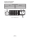
Data transfer is byte-oriented and may be shifted in 1, 2 or 3-byte patterns. One byte (8 bits) accesses the C
or configuration register, two bytes (16 bits) access the R register and 3 bytes (24 bits) access the A
register.
Internally the synthesizer has three counters used as frequency dividers. These counters are the R,A and N
counters. The R counter is actually controlled by 3 bits of the R register while the remaining 13 bits
determine the divide by R value. The frequency at pin 20 (12.8 MHz) is divided by R to determine the
frequency steps of the PLL synthesizer. In programming the radio, 5.0 kHz or 6.250 kHz step sizes can be
selected for any channel.
The 24- bit A register controls the N and A (prescaler) counts. Together these counts determine the total
synthesizer divide ratio affecting the f
in
(frequency input) signal from the VCO. A0-A7 are the A counter
values. A8-A19 are the N counter values. A21 and A20 must always be set high. A23 and A22 are both
set to 0 which controls the function of output A and causes it to be a port. This port, output A, is used to set
TX power high or low. A high output on port A sets transmit power low.
The 8-bit C register performs control functions as stated:
C7 sets polarity of the phase detector bits. Logic “0” is normal.
C6 determines the phase detector used. A logic “0” selects theta V and theta R outputs
C5 enables the lock detector when its logic is “1”.
C4 when a logic “1”, puts CMOS sections in standby mode.
C3 and C2 set phase detector current at the PD output. Not used in this application.
C1 is the value present at Output A.
C0 is the value present at Output B.
Transistors Q101 through Q104, along with related resistors and capacitors, connect the dual pin theta V
and Theta R outputs intoa2mAcurrent source that is powered by a 20V DC to DC converter. This allows
the tuning voltage to be approximately 3 to 17 VDC.
MAXON SM-2000 MOBILE
THEORY OF OPERATION
Page-13-
December 98