


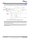
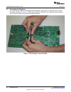
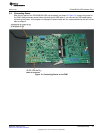
System Setup
www.ti.com
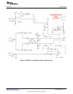
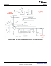
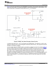
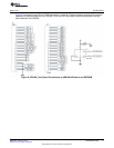
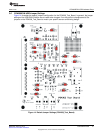
2.4 PGA309_Test_Board: Signal Definitions and Pinouts
This section provides the signal definitions for the PGA309_Test_Board.
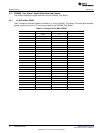
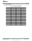
2.4.1 J1 (25-Pin Male DSUB)
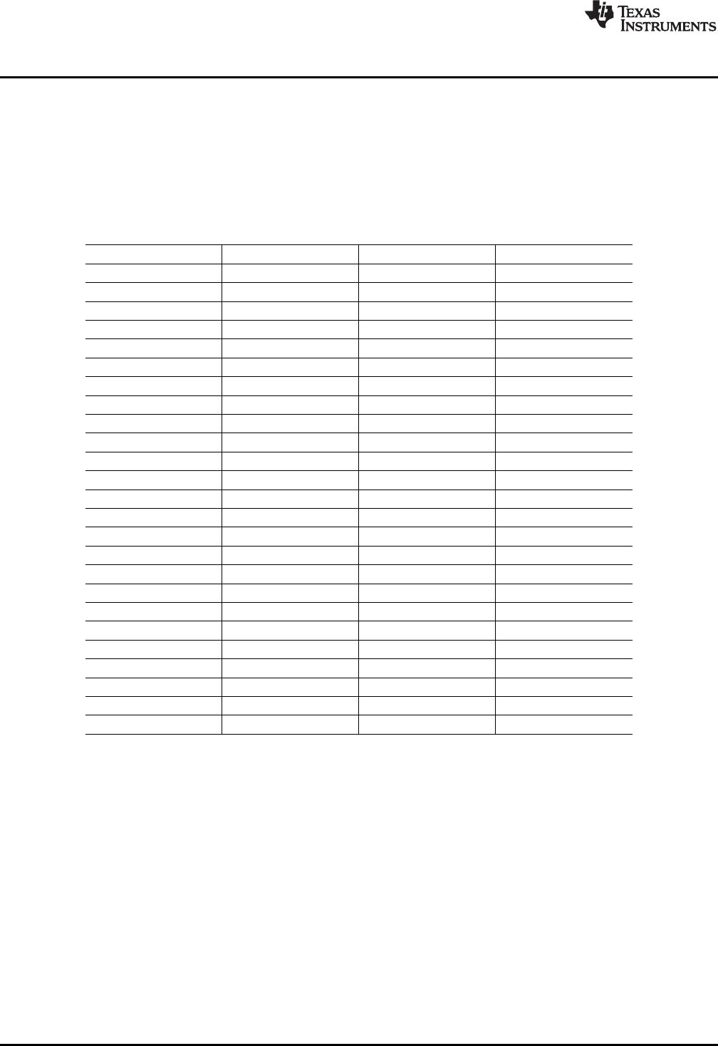
Table 2 shows the different signals connected to J1 on the PGA309_Test_Board. This table also identifies
signals connected to pins on J1 that are not used on the PGA309_Test_Board.
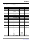
Table 2. J1 Pinout (25-Pin Male DSUB)
Pin on J1 Signal Used on This EVM PGA309 Pin
1 DAC A No
2 DAC B No
3 DAC C No
4 DAC D No
5 ADS1+ No
6 ADS1- No
7 ADS2+ No
8 ADS2– No
9 I2C_SCK No
10 I2C_SDA2 No
11 ONE_WIRE No
12 I2C_SCK_ISO Yes SCL
13 I2C_SDA_ISO Yes SDA
14 XTR_LOOP+ No
15 XTR_LOOP– No
16 INA– No
17 V
DUT
Yes V
S
18 V
CC
No
19 +15v No
20 –15v No
21 GND Yes GND
22 SPI_SCK No
23 SPI_CS1 No
24 SPI_DOUT No
25 SPI_DIN1 No
14
PGA309EVM-USB SBOU084–February 2010
Submit Documentation Feedback
Copyright © 2010, Texas Instruments Incorporated