System Setup
www.ti.com
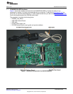
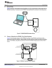
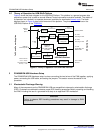
The PGA309_Test_Board also has an onboard sensor emulator. The sensor emulator is a circuit that
generates the same type of signals generated by a bridge sensor. The sensor emulator circuit is controlled
by the PGA309EVM-USB software. Using the sensor emulator allows you to get a deeper understanding
of the PGA309EVM-USB software and hardware more quickly. When the capabilities and functions of the
PGA309EVM-USB are fully understood, you can connect the real-world sensor to the EVM and perform a
full calibration.
Note that calibrations with real-world sensors are time-consuming because devices such as these are
normally calibrated at multiple temperatures in an environmental chamber. It is not unusual for
temperature calibration to require 12 hours.
2.2 PGA309_Test_Board Connections
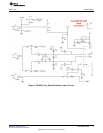
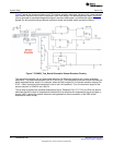
See Figure 4 for the input connections on the PGA309_Test_Board schematic. T1 provides the power
connection for an external bridge sensor. T4 allows connections to each input of the external bridge
sensor. T5 allows connection of the external temperature sensor. JMP7, JMP4, JMP5, and JMP6 allow
users to select either the onboard sensor emulator or an external sensor. JMP12 allows users to choose
between V
S
or V
EXC
for the sensor power.
The input is filtered with R3, R4, C14, C15, and C16. Note that C14 is ten times larger then C15, and C16
is used for good ac common-mode rejection. The cutoff frequency of this filter is 40.6Hz (f = 1/(2 p R3
C14)). This input filter is recommended in your final design if you have available board space.
V
EXC
has a 100pF capacitor and TEMPin has a 1nF capacitor. These components are also recommended
in your final design.
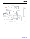
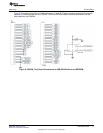
Refer to Figure 5 to see the power, reference, and digital connections on the PGA309_Test_Board
schematic. T2 provides a connection for an external reference voltage. JMP1 and JMP2 allow users to
select between the internal reference, an external reference, or power-supply reference. JMP7 and JMP8
allows users to connect the One-Wire signal to the PRG pin directly or through V
OUT
.
D2 is a transient voltage suppressor. It is useful in helping to prevent damage in an electrical overstress
(EOS) condition. R5 is useful in preventing EOS damage to the output. C6 filters noise at the output. C5
filters the reference output. These components are recommended for your design if PCB space permits.
C4 is a decoupling capacitor; it is required in the final design.
6
PGA309EVM-USB SBOU084–February 2010
Submit Documentation Feedback
Copyright © 2010, Texas Instruments Incorporated


