


TMS320 SECOND-GENERATION
DEVICES
SPRS010B — MAY 1987 — REVISED NOVEMBER 1990
POST OFFICE BOX 1443 • HOUSTON, TEXAS 77001
2
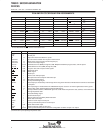
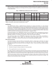
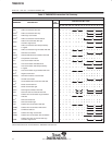
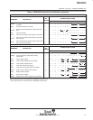
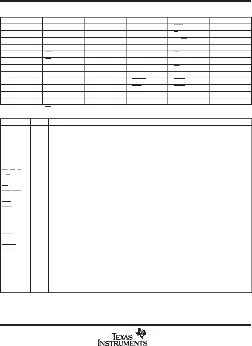
PGA AND PLCC/CER-QUAD PIN ASSIGNMENTS
FUNCTION PIN FUNCTION PIN FUNCTION PIN FUNCTION PIN FUNCTION PIN FUNCTION PIN
A0 K1/26 A12 K8/40 D2 E1/16 D14 A5/3 INT2 H1/22 V
CC
H2/23
A1 K2/28 A13 L9/41 D3 D2/15 D15 B6/2 IS J11/46 V
CC
L6/35
A2 L3/29 A14 K9/42 D4 D1/14 DR J1/24 MP/MC
†
A6/1 V
SS
B1/10
A3 K3/30 A15 L10/43 D5 C2/13 DS K10/45 MSC C10/59 V
SS
K11/44
A4 L4/31 BIO B7/68 D6 C1/12 DX E11/54 PS J10/47 V
SS
L2/27
A5 K4/32 BR G11/50 D7 B2/11 FSR J2/25 READY B8/66 XF D11/56
A6 L5/33 CLKOUT1 C11/58 D8 A2/9 FSX F10/53 RS A8/65 X1 G10/51
A7 K5/34 CLKOUT2 D10/57 D9 B3/8 HOLD A7/67 R/W H11/48 X2/CLKIN F11/52
A8 K6/36 CLKR B9/64 D10 A3/7 HOLDA E10/55 STRB H10/49
A9 L7/37 CLKX A9/63 D11 B4/6 IACK B11/60 SYNC F2/19
A10 K7/38 D0 F1/18 D12 A4/5 INT0 G1/20 V
CC
A10/61
A11 L8/39 D1 E2/17 D13 B5/4 INT1 G2/21 V
CC
B10/62
†
On the TMS32020, MP/MC must be connected to V
CC
.
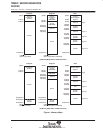
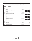
SIGNALS
I/O/Z
‡
DEFINITION
V
CC
V
SS
X1
X2/CLKIN
CLKOUT1
CLKOUT2
D15-D0
A15-A0
PS
, DS, IS
R/W
STRB
RS
INT2-INT0
MP/MC
MSC
IACK
READY
BR
XF
HOLD
HOLDA
SYNC
BIO
DR
CLKR
FSR
DX
CLKX
FSX
I
I
O
I
O
O
I/O/Z
O/Z
O/Z
O/Z
O/Z
I
I
I
O
O
I
O
O
I
O
I
I
I
I
I
O/Z
I
I/O/Z
5-V supply pins
Ground pins
Output from internal oscillator for crystal
Input to internal oscillator from crystal or external clock
Master clock output (crystal or CLKIN frequency/4)
A second clock output signal
16-bit data bus D15 (MSB) through D0 (LSB). Multiplexed between program, data, and I/O spaces.
16-bit address bus A15 (MSB) through A0 (LSB)
Program, data, and I/O space select signals
Read/write signal
Strobe signal
Reset input
External user interrupt inputs
Microprocessor/microcomputer mode select pin
Microstate complete signal
Interrupt acknowledge signal
Data ready input. Asserted by external logic when using slower devices to indicate that the current bus transaction
is complete.
Bus request signal. Asserted when the TMS320C2x requires access to an external global data memory space.
External flag output (latched software-programmable signal)
Hold input. When asserted, TMS320C2x goes into an idle mode and places the data, address, and control lines in
the high impedance state.
Hold acknowledge signal
Synchronization input
Branch control input. Polled by BIOZ instruction.
Serial data receive input
Clock for receive input for serial port
Frame synchronization pulse for receive input
Serial data transmit output
Clock for transmit output for serial port
Frame synchronization pulse for transmit. Configuration as either an input or an output.
‡
I/O/Z denotes input/output/high-impedance state.